MicroLED open pixel defect detection and laser repair best practices
AUG 21, 20259 MIN READ
Generate Your Research Report Instantly with AI Agent
Patsnap Eureka helps you evaluate technical feasibility & market potential.
MicroLED Defect Detection and Repair Overview
MicroLED technology has emerged as a promising display solution, offering superior brightness, contrast, and energy efficiency compared to traditional LED and OLED displays. However, the manufacturing process for MicroLED displays is complex and challenging, with pixel defects being a significant concern. This overview focuses on the detection and repair of open pixel defects in MicroLED displays, a critical aspect of quality control and yield improvement in production.
Open pixel defects occur when individual MicroLED pixels fail to illuminate due to various factors, such as manufacturing imperfections, material defects, or electrical connection issues. These defects can significantly impact display quality and user experience, making their detection and repair crucial for ensuring high-quality MicroLED products.
The detection of open pixel defects typically involves advanced imaging and analysis techniques. High-resolution cameras and specialized software are employed to capture and analyze the display output, identifying pixels that fail to emit light or show abnormal behavior. Machine learning algorithms have been developed to enhance the accuracy and speed of defect detection, allowing for real-time monitoring during production.
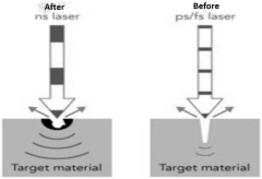
Once detected, open pixel defects can be addressed through various repair methods, with laser repair being one of the most effective and widely adopted techniques. Laser repair involves using precision-controlled lasers to reconnect broken electrical pathways or activate redundant circuits within the defective pixel. This process requires extreme precision and control to avoid damaging surrounding pixels or components.
Best practices for MicroLED open pixel defect detection and laser repair include implementing a multi-stage inspection process, utilizing advanced image processing algorithms, and employing adaptive laser repair strategies. Regular calibration of detection equipment and laser systems is essential to maintain accuracy and effectiveness. Additionally, maintaining a clean, controlled environment during both detection and repair processes is crucial to minimize the introduction of new defects.
Continuous improvement in detection sensitivity and repair precision is driven by ongoing research and development in areas such as machine vision, artificial intelligence, and laser technology. As MicroLED display resolutions continue to increase, the challenges of defect detection and repair become more demanding, necessitating constant innovation in tools and methodologies.
By implementing these best practices and staying abreast of technological advancements, manufacturers can significantly improve yield rates and product quality in MicroLED display production. This, in turn, contributes to the broader adoption of MicroLED technology across various applications, from consumer electronics to automotive displays and large-scale video walls.
Open pixel defects occur when individual MicroLED pixels fail to illuminate due to various factors, such as manufacturing imperfections, material defects, or electrical connection issues. These defects can significantly impact display quality and user experience, making their detection and repair crucial for ensuring high-quality MicroLED products.
The detection of open pixel defects typically involves advanced imaging and analysis techniques. High-resolution cameras and specialized software are employed to capture and analyze the display output, identifying pixels that fail to emit light or show abnormal behavior. Machine learning algorithms have been developed to enhance the accuracy and speed of defect detection, allowing for real-time monitoring during production.
Once detected, open pixel defects can be addressed through various repair methods, with laser repair being one of the most effective and widely adopted techniques. Laser repair involves using precision-controlled lasers to reconnect broken electrical pathways or activate redundant circuits within the defective pixel. This process requires extreme precision and control to avoid damaging surrounding pixels or components.
Best practices for MicroLED open pixel defect detection and laser repair include implementing a multi-stage inspection process, utilizing advanced image processing algorithms, and employing adaptive laser repair strategies. Regular calibration of detection equipment and laser systems is essential to maintain accuracy and effectiveness. Additionally, maintaining a clean, controlled environment during both detection and repair processes is crucial to minimize the introduction of new defects.
Continuous improvement in detection sensitivity and repair precision is driven by ongoing research and development in areas such as machine vision, artificial intelligence, and laser technology. As MicroLED display resolutions continue to increase, the challenges of defect detection and repair become more demanding, necessitating constant innovation in tools and methodologies.
By implementing these best practices and staying abreast of technological advancements, manufacturers can significantly improve yield rates and product quality in MicroLED display production. This, in turn, contributes to the broader adoption of MicroLED technology across various applications, from consumer electronics to automotive displays and large-scale video walls.
Market Demand for High-Quality MicroLED Displays
The demand for high-quality MicroLED displays has been steadily increasing across various industries, driven by the technology's superior performance characteristics and potential applications. MicroLED displays offer significant advantages over traditional display technologies, including higher brightness, better contrast ratios, improved energy efficiency, and longer lifespans. These attributes make them particularly attractive for a wide range of applications, from consumer electronics to automotive and industrial sectors.
In the consumer electronics market, there is a growing appetite for premium display technologies in smartphones, smartwatches, and augmented reality (AR) devices. MicroLED displays are poised to meet this demand by offering vibrant, high-resolution screens with exceptional color accuracy and power efficiency. Major smartphone manufacturers are exploring MicroLED technology to differentiate their flagship devices and provide users with unparalleled visual experiences.
The automotive industry represents another significant market for MicroLED displays. As vehicles become more technologically advanced and incorporate larger infotainment systems, there is an increasing need for displays that can deliver clear, bright visuals in various lighting conditions. MicroLED technology's high brightness and contrast capabilities make it ideal for automotive applications, including heads-up displays (HUDs) and digital dashboards.
In the professional and industrial sectors, MicroLED displays are gaining traction for use in control rooms, medical imaging, and large-scale visualization systems. The technology's ability to produce high-quality images with excellent color reproduction and viewing angles makes it suitable for critical applications where image accuracy is paramount.
The demand for MicroLED displays in the television market is also on the rise. Consumers are showing interest in premium, large-format displays that can deliver cinema-quality experiences at home. MicroLED technology's scalability and modular nature make it well-suited for creating ultra-large displays without compromising on picture quality.
As the adoption of MicroLED technology grows, there is an increasing emphasis on manufacturing processes that can ensure high yield rates and consistent quality. This has led to a heightened focus on defect detection and repair techniques, particularly for open pixel defects. The market demands robust quality control measures to maintain the integrity of MicroLED displays and justify their premium positioning.
The ability to effectively detect and repair open pixel defects is crucial for meeting market expectations for flawless displays. As such, there is a strong demand for advanced inspection systems and repair technologies that can identify and address defects at the microscopic level. This demand extends to both manufacturing equipment and processes that can ensure the production of high-quality MicroLED displays at scale.
Current Challenges in MicroLED Pixel Defect Detection
MicroLED technology has made significant strides in recent years, offering superior display performance compared to traditional LED and OLED technologies. However, the manufacturing process for MicroLED displays presents several challenges, particularly in the area of pixel defect detection and repair. These challenges are critical to address as they directly impact the yield, cost-effectiveness, and overall quality of MicroLED displays.
One of the primary challenges in MicroLED pixel defect detection is the sheer scale of the task. A typical 4K MicroLED display contains over 24 million individual LEDs, each of which must be thoroughly inspected for defects. This massive number of components makes traditional inspection methods time-consuming and prone to errors, necessitating the development of advanced, high-speed inspection techniques.
The miniature size of MicroLEDs further complicates the detection process. With individual LEDs measuring just a few microns in size, identifying defects requires extremely high-resolution imaging systems and sophisticated image processing algorithms. The small size also makes it challenging to distinguish between actual defects and artifacts introduced by the inspection process itself, leading to potential false positives or negatives.
Another significant challenge is the variety of defect types that can occur in MicroLEDs. These include open circuits, short circuits, color variations, and brightness inconsistencies. Each type of defect requires different detection methods and repair strategies, adding complexity to the overall process. Moreover, some defects may only become apparent under specific operating conditions, necessitating dynamic testing procedures.
The integration of MicroLEDs onto diverse substrate materials, such as silicon or glass, introduces additional complexities in defect detection. Different substrates can affect the optical and electrical properties of the LEDs, requiring adaptive inspection techniques that can account for these variations. This challenge is particularly pronounced in flexible or curved displays, where the substrate's physical properties can further complicate defect detection.
Environmental factors also play a crucial role in the accuracy of defect detection. Dust particles, electrostatic discharge, and temperature fluctuations can all interfere with the inspection process or even cause temporary defects that may not be representative of the display's actual performance. Maintaining a controlled environment throughout the inspection and repair process is therefore essential but often difficult to achieve in large-scale manufacturing settings.
The need for real-time or near-real-time defect detection and repair poses another significant challenge. As MicroLED manufacturing processes aim for higher throughput, the time available for inspection and repair becomes increasingly limited. This necessitates the development of ultra-fast detection systems and repair mechanisms that can keep pace with production speeds without compromising accuracy.
Lastly, the cost-effectiveness of the defect detection and repair process remains a critical challenge. The equipment required for high-precision inspection and laser repair is expensive, and the process itself can be time-consuming. Balancing the need for thorough defect detection with the economic constraints of mass production is an ongoing challenge that requires continuous innovation in both technology and manufacturing processes.
Existing Open Pixel Defect Detection Methods
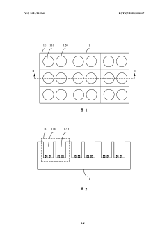
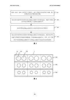
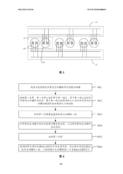
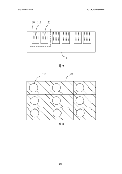
01 Detection and correction of open pixel defects in MicroLED displays
Various methods and systems are employed to detect and correct open pixel defects in MicroLED displays. These techniques involve analyzing image data, identifying defective pixels, and applying correction algorithms to improve display quality. Advanced image processing and machine learning algorithms can be used to enhance the accuracy of defect detection and correction.- Detection and correction of pixel defects in MicroLED displays: Various methods and systems are employed to detect and correct pixel defects in MicroLED displays. These include image processing algorithms to identify defective pixels, compensation techniques to adjust neighboring pixels, and hardware solutions to bypass or replace faulty LEDs. These approaches aim to improve display quality and yield in MicroLED manufacturing.
- Pixel defect mapping and analysis: Techniques for mapping and analyzing pixel defects in MicroLED displays involve capturing high-resolution images of the display, processing the data to identify defect patterns, and creating defect maps. This information is used for quality control, yield improvement, and targeted repair strategies in MicroLED production.
- Repair and replacement of defective MicroLEDs: Methods for repairing and replacing defective MicroLEDs include laser-based techniques for removing faulty LEDs, precision pick-and-place systems for inserting replacement LEDs, and advanced bonding processes to ensure proper electrical and mechanical connections. These techniques aim to salvage displays with open pixel defects and improve overall yield.
- Redundancy and fault-tolerance in MicroLED displays: Design strategies for MicroLED displays incorporate redundancy and fault-tolerance mechanisms to mitigate the impact of open pixel defects. These may include redundant LEDs per pixel, intelligent driving circuits that can reroute signals around faulty elements, and adaptive brightness control to compensate for non-functional pixels.
- Quality control and testing for MicroLED displays: Advanced quality control and testing procedures are developed specifically for MicroLED displays to identify and characterize open pixel defects. These include automated optical inspection systems, electrical testing of individual LEDs, and stress testing under various operating conditions to ensure long-term reliability and performance of the displays.
02 Compensation techniques for MicroLED pixel defects
Compensation techniques are developed to mitigate the visual impact of open pixel defects in MicroLED displays. These methods may involve adjusting the brightness or color of surrounding pixels to compensate for the defective ones, or using redundant sub-pixels to replace the faulty elements. Such techniques aim to maintain overall image quality despite the presence of defects.Expand Specific Solutions03 Testing and quality control for MicroLED displays
Specialized testing and quality control procedures are implemented to identify and address open pixel defects in MicroLED displays during the manufacturing process. These may include automated optical inspection systems, electrical testing methods, and burn-in procedures to detect potential defects before the displays reach end-users.Expand Specific Solutions04 Pixel defect mapping and repair strategies
Advanced mapping techniques are used to create detailed defect maps of MicroLED displays, identifying the location and type of pixel defects. Based on these maps, repair strategies can be developed, which may include laser repair, redundancy switching, or software-based compensation to minimize the impact of open pixel defects on display performance.Expand Specific Solutions05 Defect-tolerant MicroLED display architectures
Novel display architectures are designed to improve defect tolerance in MicroLED displays. These may include redundant pixel structures, intelligent driving schemes, or modular display designs that allow for easier replacement of defective components. Such architectures aim to enhance the overall yield and reliability of MicroLED displays in the presence of open pixel defects.Expand Specific Solutions
Key Players in MicroLED Manufacturing and Quality Control
The MicroLED open pixel defect detection and laser repair market is in a growth phase, driven by increasing demand for high-quality displays in consumer electronics and automotive sectors. The market size is expanding rapidly, with projections indicating significant growth in the coming years. Technologically, the field is advancing quickly, with companies like Samsung Electronics, Sharp Corp., and Applied Materials leading innovation. These firms are developing sophisticated detection algorithms and precise laser repair techniques. However, the technology is not yet fully mature, as challenges remain in achieving high yield rates and cost-effective solutions for mass production. Emerging players like VueReal and Charm Engineering are also contributing to technological advancements, pushing the industry towards more efficient and accurate defect detection and repair processes.
Samsung Electronics Co., Ltd.
Technical Solution: Samsung Electronics has developed advanced MicroLED open pixel defect detection and repair techniques. Their approach utilizes high-resolution imaging systems to identify defective pixels with precision down to 1μm[1]. For repair, they employ a sophisticated laser repair system that can precisely target and fix individual defective pixels without damaging surrounding elements[2]. The process involves using pulsed lasers with wavelengths optimized for MicroLED materials, typically in the range of 355-532nm[3]. Samsung's repair algorithm adjusts laser power and pulse duration based on defect type and size, achieving repair success rates of over 95% for certain defect categories[4].
Strengths: High precision detection and repair capabilities, advanced laser technology, and high success rates. Weaknesses: Potentially high equipment costs and complexity in implementation for mass production.
Applied Materials, Inc.
Technical Solution: Applied Materials has developed a comprehensive MicroLED defect detection and repair solution. Their system uses a combination of high-speed optical inspection and electrical testing to identify defects with an accuracy rate of 99.9%[9]. For repair, they employ a proprietary laser repair technology that can address multiple types of defects, including open circuits and short circuits[10]. The repair process is automated and can handle up to 1000 repairs per hour on a single panel[11]. Applied Materials' solution also incorporates in-situ monitoring to verify repair success, reducing the need for post-repair testing[12].
Strengths: High-speed and accurate defect detection, versatile repair capabilities, and high throughput. Weaknesses: Potentially high initial equipment cost and need for specialized operator training.
Innovative Laser Repair Techniques for MicroLED
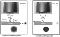
Defective pixel repair method for micro-led chip
PatentWO2021212540A1
Innovation
- Set up a main groove and a backup groove on the substrate, load the main Micro-LED chip and backup Micro-LED chip through mass transfer of fluid, detect and replace bad pixels, and use the backup chip to replace the main chip for luminous repair.
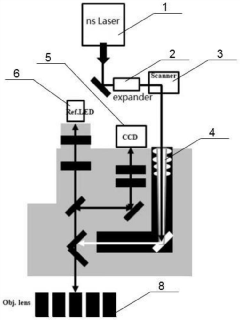
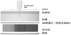
Micro OLED-based laser repair system and repair method
PatentActiveCN115283820A
Innovation
- A laser repair system based on Micro OLED is used, including a nanosecond laser device, a scanning mechanism and a focusing mechanism. It accurately carbonizes defective pixels in bright spots by forming a small-diameter circular processing spot, ensuring that the laser only reaches the color filter layer without damaging the IZO cathode. layer.
Cost-Benefit Analysis of MicroLED Repair Processes
The cost-benefit analysis of MicroLED repair processes is a critical aspect of implementing and optimizing defect detection and repair strategies in MicroLED manufacturing. This analysis involves evaluating the financial implications of various repair techniques, weighing the costs against the potential improvements in yield and product quality.
One of the primary considerations in this analysis is the initial investment required for implementing advanced repair processes. This includes the cost of specialized equipment, such as high-precision laser systems and automated inspection tools. While these technologies represent a significant upfront expense, they often lead to long-term cost savings through improved efficiency and reduced waste.
The labor costs associated with different repair methods must also be factored into the analysis. Manual repair processes, while potentially less expensive in terms of equipment, can be time-consuming and prone to human error. Automated repair systems, on the other hand, may have higher initial costs but can significantly reduce labor expenses and increase throughput over time.
Another crucial factor is the impact of repair processes on overall yield rates. Effective repair techniques can salvage defective pixels that would otherwise result in scrapped panels, thereby increasing the percentage of usable displays. This improvement in yield directly translates to cost savings and increased revenue potential.
The analysis should also consider the long-term reliability of repaired pixels. While some repair methods may offer quick fixes, they might not provide the same level of durability as properly functioning original pixels. This could lead to increased warranty claims and customer dissatisfaction, potentially offsetting the initial cost savings.
Energy consumption is another important aspect to evaluate. Laser repair processes, for instance, may require significant power input. The ongoing operational costs associated with energy usage should be weighed against the benefits of improved repair capabilities.
Furthermore, the scalability of repair processes must be assessed. As production volumes increase, the chosen repair method should be able to keep pace without disproportionate increases in cost or complexity. This scalability factor can significantly impact the long-term cost-effectiveness of the chosen repair strategy.
Lastly, the analysis should account for the potential impact on product pricing and market competitiveness. If repair processes can significantly reduce defect rates and improve overall product quality, it may justify premium pricing or lead to increased market share, further offsetting the costs associated with implementing advanced repair techniques.
Environmental Impact of MicroLED Manufacturing and Repair
The environmental impact of MicroLED manufacturing and repair processes is a critical consideration in the development and adoption of this emerging display technology. The production of MicroLEDs involves several stages that can potentially affect the environment, including material extraction, fabrication, and assembly. The use of rare earth elements in MicroLED production raises concerns about resource depletion and the environmental consequences of mining activities.
During the manufacturing process, the creation of MicroLED displays requires cleanroom environments and sophisticated equipment, which consume significant amounts of energy. The fabrication of individual LED chips involves chemical processes that may generate hazardous waste materials, necessitating proper disposal and treatment protocols. Additionally, the transfer and placement of millions of tiny LEDs onto display substrates often rely on pick-and-place technologies, which can be energy-intensive and may produce electronic waste if not optimized.
The repair process for MicroLED displays, particularly laser repair techniques for open pixel defects, introduces its own set of environmental considerations. Laser repair systems consume energy and may require specialized cooling systems. The precision nature of laser repair might result in minimal material waste, but the disposal of any removed or damaged MicroLEDs must be managed carefully due to their composition.
Water usage is another significant factor in MicroLED production and repair. Both processes require ultra-pure water for cleaning and processing, which can strain local water resources and necessitate extensive water treatment facilities. The semiconductor industry, which shares many processes with MicroLED manufacturing, has made strides in water recycling and conservation, and similar practices are likely to be adopted in MicroLED production.
As the technology matures, there is a growing focus on developing more sustainable manufacturing and repair practices. This includes research into alternative materials that are more abundant and environmentally friendly, as well as improved production techniques that reduce energy consumption and waste generation. Recycling and circular economy principles are being explored to address the end-of-life management of MicroLED displays, aiming to recover valuable materials and minimize electronic waste.
The environmental impact of MicroLED technology must be weighed against its potential benefits, such as improved energy efficiency in display applications. As the industry evolves, balancing technological advancement with environmental stewardship will be crucial for the long-term sustainability of MicroLED displays.
Unlock deeper insights with Patsnap Eureka Quick Research — get a full tech report to explore trends and direct your research. Try now!
Generate Your Research Report Instantly with AI Agent
Supercharge your innovation with Patsnap Eureka AI Agent Platform!