MicroLED transfer printing vs wafer bonding: cost and yield trade-offs
AUG 21, 20259 MIN READ
Generate Your Research Report Instantly with AI Agent
Patsnap Eureka helps you evaluate technical feasibility & market potential.
MicroLED Transfer Tech Evolution and Objectives
MicroLED technology has emerged as a promising candidate for next-generation displays, offering superior brightness, contrast, and energy efficiency compared to traditional LED and OLED technologies. The evolution of MicroLED transfer techniques has been driven by the need to overcome challenges in manufacturing scalability and cost-effectiveness.
The primary objective of MicroLED transfer technology is to efficiently and accurately place millions of tiny LED chips onto a display substrate. This process is critical for achieving high-resolution displays while maintaining production yields and reducing costs. Two main approaches have emerged in this field: transfer printing and wafer bonding.
Transfer printing, initially developed in the early 2000s, involves selectively picking up and placing individual MicroLED chips from a donor wafer onto a receiving substrate. This technique has evolved to include various methods such as stamp-based transfer, laser-assisted transfer, and electrostatic transfer. The goal is to improve transfer speed, accuracy, and yield while minimizing damage to the delicate MicroLED structures.
Wafer bonding, on the other hand, aims to transfer entire arrays of MicroLEDs simultaneously. This technique involves bonding a wafer containing MicroLED arrays to a display backplane, followed by substrate removal. The evolution of wafer bonding has focused on enhancing bonding strength, improving alignment accuracy, and developing methods for selective transfer of specific regions.
Both transfer printing and wafer bonding techniques have seen significant advancements over the past decade. Researchers and industry players have been working to optimize these processes for mass production, with the ultimate goal of making MicroLED displays commercially viable for a wide range of applications, from smartphones and smartwatches to large-scale displays and augmented reality devices.
The ongoing evolution of these transfer technologies aims to address several key objectives. First, improving transfer yield is crucial for reducing production costs and increasing manufacturing efficiency. Second, enhancing the precision and reliability of the transfer process is essential for producing high-quality displays with uniform performance. Third, scaling up the transfer process to handle larger substrate sizes and higher throughput is necessary for meeting the demands of various display applications.
As the MicroLED industry continues to mature, the focus on transfer technology evolution remains critical. The trade-offs between cost and yield in transfer printing versus wafer bonding approaches represent a key area of research and development. Future advancements in these technologies will play a pivotal role in determining the widespread adoption and commercial success of MicroLED displays across diverse market segments.
Market Demand for MicroLED Displays
The market demand for MicroLED displays has been steadily growing, driven by the technology's potential to revolutionize various display applications. MicroLED offers several advantages over existing display technologies, including higher brightness, better contrast ratios, improved energy efficiency, and longer lifespans. These benefits have sparked interest across multiple industries, particularly in consumer electronics, automotive, and professional display markets.
In the consumer electronics sector, smartphones and smartwatches are expected to be early adopters of MicroLED technology. The demand for high-quality, power-efficient displays in these devices aligns well with MicroLED's capabilities. Major smartphone manufacturers are investing heavily in MicroLED research and development, anticipating a shift towards this technology in premium devices.
The automotive industry represents another significant market for MicroLED displays. As vehicles become more technologically advanced, there is an increasing need for high-performance, durable displays for infotainment systems, heads-up displays, and digital dashboards. MicroLED's ability to deliver bright, clear images even in direct sunlight makes it particularly attractive for automotive applications.
Professional display markets, including broadcast studios, control rooms, and large-scale digital signage, are also showing strong interest in MicroLED technology. The demand for high-resolution, large-format displays with exceptional image quality is driving adoption in these sectors. MicroLED's scalability and modular nature make it well-suited for creating massive display walls and screens of various sizes and shapes.
The augmented reality (AR) and virtual reality (VR) markets present another avenue for MicroLED growth. As these technologies advance, there is a growing need for compact, high-resolution displays with low power consumption. MicroLED's characteristics make it a promising candidate for next-generation AR/VR headsets, potentially addressing current limitations in display quality and energy efficiency.
While the potential market for MicroLED displays is substantial, widespread adoption faces challenges related to manufacturing costs and production yields. The industry is actively working to overcome these hurdles, with significant investments being made in improving transfer printing and wafer bonding techniques. As these processes are refined and economies of scale are achieved, the cost of MicroLED displays is expected to decrease, further driving market demand.
The global pandemic has also influenced market dynamics, accelerating the adoption of digital technologies and remote communication tools. This trend has increased the demand for high-quality displays across various applications, from home entertainment systems to professional video conferencing setups, potentially benefiting MicroLED technology in the long term.
Current Challenges in MicroLED Transfer Methods
MicroLED transfer methods face several significant challenges that impact both cost and yield in the manufacturing process. One of the primary issues is the precision required for mass transfer of microscopic LED chips. The transfer process demands extremely high accuracy, often at the micron level, to ensure proper alignment and placement of each individual LED on the target substrate.
The fragility of MicroLED chips presents another major challenge. These tiny devices are susceptible to damage during the transfer process, which can lead to reduced yield and increased production costs. The delicate nature of MicroLEDs requires careful handling and innovative transfer techniques to minimize damage and maintain high yield rates.
Scalability remains a significant hurdle for MicroLED transfer methods. As display sizes increase and pixel densities become higher, the number of MicroLEDs that need to be transferred grows exponentially. This scaling challenge puts pressure on transfer equipment to maintain speed and accuracy while handling an ever-increasing number of devices.
The issue of defect management is also critical in MicroLED transfer. Even a small number of defective or misplaced LEDs can result in visible imperfections in the final display. Developing robust defect detection and repair mechanisms is essential for maintaining high yield rates and ensuring product quality.
Transfer speed is another key challenge that directly impacts production costs. Current transfer methods often struggle to achieve the high throughput necessary for cost-effective mass production of MicroLED displays. Balancing transfer speed with precision and yield is a complex optimization problem that manufacturers must solve.
The choice between transfer printing and wafer bonding methods involves trade-offs in terms of cost and yield. Transfer printing offers flexibility in handling different chip sizes and can be more cost-effective for smaller production runs. However, it may face challenges in maintaining consistent yield for large-scale production. Wafer bonding, on the other hand, can potentially offer higher throughput and yield for large-scale production but may be less flexible and have higher initial equipment costs.
Addressing these challenges requires ongoing research and development in areas such as advanced pick-and-place technologies, innovative adhesive materials, and improved process control systems. The industry is actively exploring solutions like laser-assisted transfer, fluidic self-assembly, and electrostatic transfer to overcome these hurdles and make MicroLED production more efficient and cost-effective.
Transfer Printing vs Wafer Bonding Techniques
01 Manufacturing process optimization
Improving manufacturing processes to reduce costs and increase yield of MicroLED production. This includes developing more efficient transfer and bonding techniques, optimizing epitaxial growth processes, and implementing advanced quality control measures throughout the production line.- Manufacturing process optimization: Improving manufacturing processes is crucial for reducing MicroLED costs and increasing yield. This includes developing more efficient transfer and bonding techniques, optimizing epitaxial growth processes, and implementing advanced quality control measures. Automation and precision engineering play key roles in enhancing production efficiency and reducing defects.
- Material innovations: Advancements in materials used for MicroLED production can significantly impact cost and yield. This involves developing new substrate materials, improving LED epitaxial structures, and creating more efficient phosphors and color conversion materials. Novel materials can enhance light output, reduce power consumption, and improve overall device performance.
- Defect detection and repair: Implementing advanced defect detection and repair techniques is essential for improving MicroLED yield. This includes developing high-resolution inspection systems, machine learning algorithms for defect identification, and innovative repair methods such as laser-based techniques or redundancy strategies. Effective defect management can significantly reduce waste and increase production efficiency.
- Scaling and miniaturization: Efforts to scale up production while simultaneously miniaturizing MicroLED components are critical for cost reduction. This involves developing new lithography techniques, improving chip design for higher density, and creating more efficient packaging methods. Miniaturization can lead to more displays per wafer, reducing overall production costs.
- Integration and testing innovations: Advancements in integration and testing processes can significantly impact MicroLED cost and yield. This includes developing more efficient methods for integrating MicroLEDs with driving circuits, creating innovative testing protocols for rapid performance assessment, and implementing in-line monitoring systems. Improved integration and testing can reduce assembly time and increase overall product quality.
02 Material selection and development
Focusing on the selection and development of cost-effective materials for MicroLED fabrication. This involves researching alternative substrate materials, improving LED epitaxial structures, and developing novel phosphor materials to enhance efficiency and reduce overall production costs.Expand Specific Solutions03 Defect detection and repair techniques
Implementing advanced defect detection and repair techniques to improve yield rates. This includes developing high-resolution inspection systems, machine learning algorithms for defect identification, and innovative repair methods such as laser-based pixel correction.Expand Specific Solutions04 Mass transfer technology advancements
Developing and improving mass transfer technologies to enable efficient and precise placement of large numbers of MicroLEDs. This involves creating specialized equipment and processes for handling and transferring microscopic LED chips, as well as optimizing alignment and bonding techniques.Expand Specific Solutions05 Integration of automated systems
Incorporating automated systems and Industry 4.0 concepts into MicroLED production lines to reduce labor costs and improve consistency. This includes implementing robotics, AI-driven process control, and real-time monitoring systems to optimize production efficiency and yield.Expand Specific Solutions
Key Players in MicroLED Manufacturing
The MicroLED transfer printing vs wafer bonding technology competition is in an early growth stage, with the market expected to expand significantly in the coming years. The global MicroLED market size is projected to reach billions of dollars by 2025, driven by demand for high-performance displays. While the technology is still maturing, several key players are making advancements. Companies like Apple, Samsung, and BOE are investing heavily in MicroLED R&D and manufacturing capabilities. Smaller specialized firms like eLux and X Display Co. are also contributing innovations. The industry is working to improve yields and reduce costs to enable mass production and wider adoption across various applications.
BOE Technology Group Co., Ltd.
Technical Solution: BOE has been actively developing both MicroLED transfer printing and wafer bonding technologies. For large displays, BOE employs a mass transfer technique using a proprietary "adhesive-free" method that reduces the risk of contamination during the transfer process[12]. This approach allows for the simultaneous transfer of thousands of MicroLEDs. For smaller displays, BOE has explored a hybrid bonding technique that combines aspects of wafer bonding and transfer printing. The company has also invested in developing high-precision pick-and-place equipment for individual MicroLED transfer, which offers flexibility for repairing defects and creating displays with non-standard pixel arrangements[13]. BOE's research focuses on improving transfer yield and reducing costs through process optimization and automation.
Strengths: Diverse range of transfer technologies suitable for various display sizes, innovative "adhesive-free" approach. Weaknesses: May face challenges in scaling up production to compete with more established players in the MicroLED market.
Apple, Inc.
Technical Solution: Apple has developed a proprietary MicroLED transfer printing technology for its future displays. Their approach involves using a temporary carrier wafer to transfer and precisely place individual MicroLED pixels onto a target substrate[1]. This method allows for selective transfer of only known-good LEDs, potentially improving yield. Apple's process utilizes laser-assisted transfer, where a laser pulse heats an interface layer to release LEDs from the carrier[2]. The company has also explored hybrid approaches combining aspects of transfer printing and wafer bonding to optimize for different display sizes and applications[3].
Strengths: Highly precise pixel placement, potential for improved yield through selective transfer. Weaknesses: Complex process requiring specialized equipment, potentially higher cost for small-scale production.
Core Innovations in MicroLED Transfer
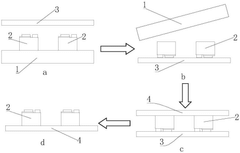
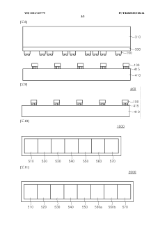
Micro-LED mass transfer and bonding method
PatentPendingCN119317278A
Innovation
- Using laser peeling and film transfer technology, large-area peeling of the Micro-LED array is achieved through laser peeling, and the difference in viscosity of the film is used to peel the Micro-LED array from the substrate and transfer it to the flexible film through multiple flips. High-speed, high-yield mass transfer process.
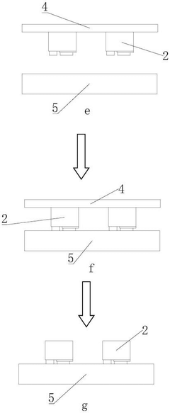
Micro-led transfer method and micro-led transfer apparatus
PatentWO2021125775A1
Innovation
- A micro LED transfer method and device that uses a first adhesive material layer with a reduced adhesive force after curing, allowing micro LEDs to be transferred from a first carrier substrate to a second carrier substrate with a higher adhesive force, and then selectively bonding them to a circuit board using a metal bonding layer, while ensuring the second carrier substrate has a thermal expansion coefficient similar to the circuit board to prevent bonding defects.
Cost Analysis of Transfer Methods
The cost analysis of transfer methods for MicroLED manufacturing is a critical factor in determining the viability and scalability of this emerging display technology. Transfer printing and wafer bonding are two primary techniques used in the production process, each with its own cost implications and yield considerations.
Transfer printing, a pick-and-place method, offers flexibility in terms of pixel arrangement and substrate compatibility. However, it faces challenges in terms of equipment costs and throughput. The initial investment for transfer printing equipment can be substantial, often ranging from $5 million to $20 million per machine. These systems require precise alignment capabilities and specialized tooling, contributing to their high cost. Additionally, the process speed of transfer printing can be a limiting factor, with current systems capable of transferring thousands to tens of thousands of pixels per second.
Wafer bonding, on the other hand, presents a different cost structure. This method allows for the simultaneous transfer of large arrays of MicroLEDs, potentially offering higher throughput. The equipment costs for wafer bonding can be lower than those for transfer printing, typically ranging from $2 million to $10 million per system. However, wafer bonding may require more stringent cleanroom conditions and specialized wafer preparation processes, which can add to the overall manufacturing costs.
Yield is a crucial factor in the cost analysis of both methods. Transfer printing allows for selective pickup and placement, potentially improving yield by enabling the transfer of only known-good devices. This selective approach can reduce material waste and improve overall efficiency. However, the individual handling of MicroLEDs increases the risk of damage during transfer, potentially impacting yield.
Wafer bonding typically offers higher throughput but may face challenges in terms of yield, especially for large-area displays. Any defects or misalignments during the bonding process can affect entire arrays of MicroLEDs, potentially leading to higher scrap rates. However, advancements in wafer bonding techniques, such as temporary bonding and debonding processes, are improving yield rates and reducing associated costs.
The cost-yield trade-off between these methods is further influenced by factors such as display size, pixel density, and production volume. For smaller, high-resolution displays, transfer printing may offer advantages in terms of precision and flexibility. In contrast, wafer bonding might be more cost-effective for larger displays or high-volume production scenarios where throughput is a priority.
Yield Optimization Strategies
Yield optimization strategies play a crucial role in the production of MicroLED displays, particularly when comparing transfer printing and wafer bonding techniques. These strategies aim to maximize the number of functional devices produced while minimizing defects and waste.
For transfer printing, one key optimization strategy involves improving the accuracy and reliability of the pick-and-place process. This can be achieved through advanced machine vision systems and precise robotic control. By enhancing the alignment accuracy during transfer, the yield of successfully placed MicroLEDs can be significantly increased.
Another important strategy for transfer printing is the development of specialized adhesive materials. These materials must provide strong bonding between the MicroLEDs and the target substrate while allowing for easy release from the donor wafer. Optimizing the chemical composition and application methods of these adhesives can lead to higher transfer success rates and improved overall yield.
In the case of wafer bonding, yield optimization often focuses on improving the uniformity of the bonding process across the entire wafer surface. This can be accomplished through careful control of temperature, pressure, and surface preparation techniques. Advanced plasma activation methods and ultra-clean bonding environments can help ensure consistent bonding quality, reducing the occurrence of voids or weak interfaces that could lead to device failure.
Surface planarization is another critical strategy for wafer bonding yield improvement. By reducing surface roughness and ensuring uniform contact between the bonding surfaces, the likelihood of successful bonding increases. Chemical-mechanical polishing (CMP) and other advanced planarization techniques can be employed to achieve the required surface quality.
For both transfer printing and wafer bonding, defect detection and management are essential yield optimization strategies. Implementing in-line inspection systems using high-resolution imaging and automated defect classification can help identify and isolate problematic areas early in the production process. This allows for targeted rework or selective discarding of defective regions, minimizing the impact on overall yield.
Additionally, optimizing the design of test structures and implementing comprehensive electrical testing protocols can help identify and isolate functional devices more effectively. This is particularly important for MicroLED displays, where even small numbers of defective pixels can significantly impact product quality.
Finally, continuous process monitoring and statistical analysis play a crucial role in yield optimization for both techniques. By collecting and analyzing data on process parameters, defect rates, and yield trends, manufacturers can identify areas for improvement and implement targeted optimizations. This data-driven approach allows for ongoing refinement of the production process, leading to sustained yield improvements over time.
Unlock deeper insights with Patsnap Eureka Quick Research — get a full tech report to explore trends and direct your research. Try now!
Generate Your Research Report Instantly with AI Agent
Supercharge your innovation with Patsnap Eureka AI Agent Platform!