MicroLED mura metrology and calibration workflows for uniformity at scale
AUG 21, 20259 MIN READ
Generate Your Research Report Instantly with AI Agent
Patsnap Eureka helps you evaluate technical feasibility & market potential.
MicroLED Mura Challenges
MicroLED displays have emerged as a promising technology for next-generation displays, offering superior brightness, contrast, and energy efficiency. However, the manufacturing process for MicroLED displays faces significant challenges, particularly in achieving uniform brightness and color across the entire display. This non-uniformity, known as mura, is a critical issue that affects the overall quality and performance of MicroLED displays.
Mura defects in MicroLED displays can manifest in various forms, including brightness variations, color inconsistencies, and pixel-to-pixel differences. These defects are often caused by inherent variations in the manufacturing process, such as inconsistencies in LED chip quality, variations in the transfer and bonding processes, and differences in the electrical characteristics of individual LEDs.
One of the primary challenges in addressing MicroLED mura is the sheer scale of the problem. A typical MicroLED display contains millions of individual LED chips, each of which must be precisely controlled to achieve uniform performance. This scale makes traditional inspection and calibration methods impractical, necessitating the development of new, highly efficient metrology and calibration workflows.
Another significant challenge is the multi-dimensional nature of mura defects. Unlike traditional displays, where uniformity issues may primarily relate to brightness, MicroLED displays must contend with variations in brightness, color, and even the size and shape of individual LED chips. This complexity requires sophisticated measurement and analysis techniques that can capture and quantify these various aspects of display performance.
The dynamic nature of MicroLED displays also presents unique challenges for mura correction. The performance of individual LEDs can change over time due to factors such as temperature variations and aging effects. This means that uniformity correction must be an ongoing process, rather than a one-time calibration, adding further complexity to the metrology and calibration workflows.
Furthermore, the high-resolution nature of MicroLED displays demands extremely precise measurement and correction techniques. Even small variations in LED performance can be noticeable to the human eye, especially in applications such as augmented reality (AR) and virtual reality (VR) displays, where the screen is viewed at close range.
Addressing these challenges requires a multi-faceted approach that combines advanced measurement technologies, sophisticated data analysis algorithms, and innovative calibration techniques. This may include the development of high-speed, high-resolution imaging systems for defect detection, machine learning algorithms for pattern recognition and classification, and adaptive calibration methods that can adjust to changing display characteristics over time.
Market Demand Analysis
The market demand for MicroLED mura metrology and calibration workflows for uniformity at scale is experiencing significant growth, driven by the increasing adoption of MicroLED technology across various industries. As MicroLED displays continue to gain traction in consumer electronics, automotive displays, and large-scale digital signage, the need for efficient and accurate uniformity calibration becomes paramount.
The consumer electronics sector, particularly smartphones and smartwatches, represents a substantial portion of the market demand. Major manufacturers are investing heavily in MicroLED technology for its superior brightness, contrast, and energy efficiency. This trend is expected to accelerate as production costs decrease and yield rates improve, further driving the need for advanced metrology and calibration solutions.
In the automotive industry, MicroLED displays are becoming increasingly popular for dashboard interfaces and infotainment systems. The demand for high-quality, uniform displays in vehicles is pushing manufacturers to adopt sophisticated calibration workflows to ensure consistent performance across all units. This sector's growth is anticipated to contribute significantly to the overall market demand for MicroLED uniformity solutions.
The large-format display market, including digital signage and video walls, is another key driver of demand for MicroLED mura metrology and calibration workflows. As MicroLED technology enables the creation of seamless, bezel-free displays with exceptional image quality, the need for precise uniformity control at scale becomes critical. This is particularly important for applications in retail, advertising, and public information displays where visual consistency is crucial.
Market analysts predict that the global MicroLED display market will experience substantial growth in the coming years, with some estimates suggesting a compound annual growth rate (CAGR) of over 80% between 2021 and 2026. This rapid expansion will directly impact the demand for metrology and calibration solutions, as manufacturers seek to improve production efficiency and maintain high-quality standards.
The increasing focus on augmented reality (AR) and virtual reality (VR) technologies is also contributing to the market demand. MicroLED displays are considered a promising solution for next-generation AR/VR devices due to their high brightness and low power consumption. As these technologies advance, the need for precise uniformity calibration will become even more critical to ensure immersive and consistent user experiences.
Furthermore, the growing emphasis on sustainability and energy efficiency in display technologies aligns well with MicroLED's characteristics. This environmental consideration is likely to drive additional demand for MicroLED displays and, consequently, for advanced calibration workflows that optimize their performance and longevity.
Current Metrology Status
The current state of MicroLED mura metrology and calibration workflows for uniformity at scale presents both significant advancements and persistent challenges. Traditional metrology methods, such as optical microscopy and scanning electron microscopy (SEM), have been adapted to meet the unique requirements of MicroLED displays. However, these techniques often struggle with the high-throughput demands of large-scale production.
Advanced imaging systems, incorporating high-resolution cameras and sophisticated image processing algorithms, have emerged as a cornerstone of modern MicroLED metrology. These systems can rapidly capture and analyze the light output of individual MicroLEDs across large panels, enabling the detection of mura defects and uniformity issues. Machine learning and artificial intelligence algorithms are increasingly being integrated into these systems to enhance defect recognition and classification accuracy.
Spectroradiometers and colorimeters play a crucial role in measuring the spectral characteristics and color uniformity of MicroLED displays. These instruments have been refined to provide faster measurement speeds and higher precision, critical for maintaining consistency across large display areas. However, the challenge of accurately measuring the extremely small emission areas of individual MicroLEDs remains a significant hurdle.
In-line metrology systems have been developed to address the need for real-time quality control during the manufacturing process. These systems can perform rapid measurements without interrupting the production flow, allowing for immediate feedback and adjustments. Despite these advancements, achieving consistent measurements across different production lines and facilities remains a challenge, often requiring complex calibration procedures.
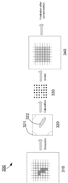
Calibration workflows have evolved to incorporate multi-step processes that address various aspects of uniformity. These typically include initial characterization, compensation calculation, and iterative refinement stages. Advanced algorithms are employed to calculate compensation matrices that can correct for variations in brightness and color across the display. However, the complexity of these workflows often results in long processing times, which can be a bottleneck in high-volume production scenarios.
The industry is increasingly moving towards integrated metrology and calibration solutions that combine multiple measurement techniques and data analysis tools. These holistic approaches aim to provide a more comprehensive assessment of display uniformity and streamline the overall quality control process. Nevertheless, the development of standardized metrology protocols for MicroLED displays is still in progress, with various industry stakeholders working towards consensus on best practices and measurement standards.
Advanced imaging systems, incorporating high-resolution cameras and sophisticated image processing algorithms, have emerged as a cornerstone of modern MicroLED metrology. These systems can rapidly capture and analyze the light output of individual MicroLEDs across large panels, enabling the detection of mura defects and uniformity issues. Machine learning and artificial intelligence algorithms are increasingly being integrated into these systems to enhance defect recognition and classification accuracy.
Spectroradiometers and colorimeters play a crucial role in measuring the spectral characteristics and color uniformity of MicroLED displays. These instruments have been refined to provide faster measurement speeds and higher precision, critical for maintaining consistency across large display areas. However, the challenge of accurately measuring the extremely small emission areas of individual MicroLEDs remains a significant hurdle.
In-line metrology systems have been developed to address the need for real-time quality control during the manufacturing process. These systems can perform rapid measurements without interrupting the production flow, allowing for immediate feedback and adjustments. Despite these advancements, achieving consistent measurements across different production lines and facilities remains a challenge, often requiring complex calibration procedures.
Calibration workflows have evolved to incorporate multi-step processes that address various aspects of uniformity. These typically include initial characterization, compensation calculation, and iterative refinement stages. Advanced algorithms are employed to calculate compensation matrices that can correct for variations in brightness and color across the display. However, the complexity of these workflows often results in long processing times, which can be a bottleneck in high-volume production scenarios.
The industry is increasingly moving towards integrated metrology and calibration solutions that combine multiple measurement techniques and data analysis tools. These holistic approaches aim to provide a more comprehensive assessment of display uniformity and streamline the overall quality control process. Nevertheless, the development of standardized metrology protocols for MicroLED displays is still in progress, with various industry stakeholders working towards consensus on best practices and measurement standards.
Existing Calibration Methods
01 Pixel structure optimization for uniformity
Improving the pixel structure of MicroLED displays to enhance uniformity. This includes optimizing the arrangement, size, and spacing of individual MicroLEDs within each pixel to achieve more consistent light output across the display. Advanced pixel designs can help mitigate issues such as color variation and brightness inconsistencies.- Improving uniformity through pixel structure design: Enhancing MicroLED uniformity by optimizing pixel structure design, including adjustments to pixel size, shape, and arrangement. This approach focuses on the physical layout of MicroLEDs to achieve more consistent light output across the display.
- Uniformity enhancement via driving circuit optimization: Addressing MicroLED uniformity issues through improvements in driving circuits and control methods. This includes developing advanced current control techniques and compensation algorithms to ensure consistent brightness across all pixels.
- Material selection and processing for uniform emission: Focusing on the selection and processing of materials used in MicroLED fabrication to achieve more uniform light emission. This involves optimizing semiconductor materials, quantum well structures, and surface treatments to reduce variations in light output.
- Transfer and bonding techniques for improved uniformity: Developing advanced transfer and bonding techniques to ensure precise placement and consistent performance of MicroLEDs. This includes innovations in mass transfer methods and substrate bonding to minimize variations in pixel positioning and electrical connections.
- Optical solutions for enhancing display uniformity: Implementing optical solutions to improve the perceived uniformity of MicroLED displays. This involves the use of micro-lenses, light diffusers, and other optical elements to distribute light more evenly and mask minor variations in individual LED performance.
02 Driving circuit and control methods
Developing sophisticated driving circuits and control methods to improve MicroLED uniformity. This involves implementing advanced algorithms for current control, voltage regulation, and timing adjustments to compensate for variations in individual MicroLED performance. Precise control over each MicroLED can significantly enhance overall display uniformity.Expand Specific Solutions03 Manufacturing process improvements
Enhancing manufacturing processes to achieve better uniformity in MicroLED production. This includes refining epitaxial growth techniques, improving transfer and bonding methods, and developing more precise etching and patterning processes. Advanced manufacturing techniques can help reduce variations in MicroLED size, shape, and performance.Expand Specific Solutions04 Substrate and material selection
Selecting appropriate substrates and materials to enhance MicroLED uniformity. This involves researching and developing new substrate materials, buffer layers, and active layer compositions that can promote more uniform MicroLED growth and performance. Optimized material choices can help reduce defects and improve overall display consistency.Expand Specific Solutions05 Compensation and calibration techniques
Implementing compensation and calibration techniques to improve MicroLED uniformity post-production. This includes developing advanced sensing and feedback systems to detect variations in MicroLED performance, coupled with software algorithms that can adjust individual MicroLED outputs in real-time. These techniques can help overcome inherent manufacturing variations and aging effects.Expand Specific Solutions
Key Industry Players
The MicroLED mura metrology and calibration market is in its growth stage, driven by increasing demand for high-quality displays in various industries. The market size is expanding rapidly, with significant investments from major players like Samsung Display, BOE Technology, and AUO Corp. Technologically, the field is advancing quickly, with companies like KLA Corp. and Mycronic AB developing sophisticated metrology and calibration solutions. However, the technology is still evolving, with challenges in achieving uniformity at scale. Emerging players like Jade Bird Display and Seoul Viosys are contributing innovative approaches, while established firms like IBM are leveraging their expertise in AI and data analytics to enhance calibration workflows. The competitive landscape is dynamic, with a mix of display manufacturers and specialized equipment providers vying for market share.
KLA Corp.
Technical Solution: KLA Corp. has developed advanced metrology and inspection solutions specifically for MicroLED displays. Their system combines high-resolution imaging with machine learning algorithms to detect and classify mura defects at the pixel level. The workflow includes automated wafer-level and panel-level inspections, with the ability to identify sub-micron defects across large areas. KLA's solution integrates with manufacturing execution systems to enable real-time process control and yield optimization[1][3]. The company has also introduced AI-powered calibration techniques that can compensate for brightness and color variations, improving overall display uniformity[2].
Strengths: Industry-leading metrology precision, comprehensive defect classification, and integration with fab systems. Weaknesses: High equipment costs and complexity may limit adoption by smaller manufacturers.
Samsung Display Co., Ltd.
Technical Solution: Samsung Display has developed a proprietary MicroLED inspection and calibration system tailored for their mass production needs. Their approach utilizes a combination of high-speed optical scanning and electrical testing to identify defects and non-uniformities. Samsung's workflow incorporates a multi-stage calibration process, including pre-transfer testing of individual LED chips and post-transfer panel-level adjustments. They have implemented an AI-driven compensation algorithm that can adjust the driving current for each MicroLED to achieve optimal uniformity across the entire display[4][5]. Samsung has also patented a method for using neighboring pixels to compensate for defective MicroLEDs, enhancing yield and reducing visible mura effects[6].
Strengths: Vertically integrated production allows for optimized workflows and rapid iteration. Extensive R&D resources. Weaknesses: Proprietary nature of the technology may limit broader industry adoption.
Core Mura Correction Tech
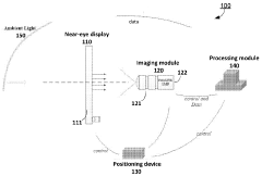
Methods and systems for MURA detection and demura
PatentWO2024020737A1
Innovation
- Development of a demura system and method specifically designed for virtual images in near-eye displays using micro LED technology.
- Addressing the unique challenges of non-uniformity in micro LED display panels, including residual images, mottled appearances, and bright or black spots.
- Improving upon conventional gray scale adjustment methods for compensating non-uniformity in micro LED displays.

Method for enhancing luminance uniformity of a display panel
PatentActiveUS20190378473A1
Innovation
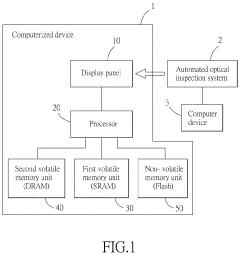
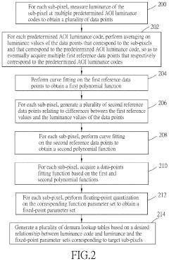
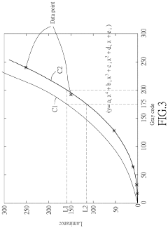
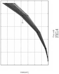
- A method involving an automated optical inspection system to measure luminance for each sub-pixel using predetermined AOI luminance codes, generating reference curves, and performing two-stage curve fitting to create data-points fitting functions, followed by floating-point quantization to obtain fixed-point parameter sets for demura operation, which are used to generate demura lookup tables for adjusting luminance codes.
Manufacturing Scalability
Manufacturing scalability is a critical aspect of MicroLED technology adoption, particularly in the context of mura metrology and calibration workflows for uniformity at scale. As the demand for high-quality displays increases, manufacturers face significant challenges in scaling up production while maintaining consistent uniformity across large panels.
One of the primary obstacles in scaling MicroLED manufacturing is the complexity of the mura metrology process. Mura, which refers to non-uniform brightness or color across a display, becomes increasingly difficult to detect and correct as panel sizes grow. Traditional inspection methods often struggle to keep pace with high-volume production, leading to bottlenecks in the manufacturing pipeline.
To address these challenges, advanced automated inspection systems are being developed. These systems utilize high-resolution cameras and sophisticated image processing algorithms to detect even subtle variations in brightness and color across large MicroLED panels. Machine learning techniques are also being employed to improve the accuracy and speed of mura detection, enabling real-time adjustments during the production process.
Calibration workflows are evolving to accommodate the demands of large-scale manufacturing. Adaptive calibration techniques are being implemented, allowing for dynamic adjustments based on real-time measurement data. This approach helps to compensate for variations in individual LED performance and ensures uniform output across the entire display surface.
Parallel processing techniques are being explored to enhance the efficiency of mura correction. By dividing large panels into smaller sections that can be calibrated simultaneously, manufacturers can significantly reduce processing times without compromising on quality. This approach is particularly beneficial for ultra-large displays used in digital signage and control room applications.
The development of standardized calibration protocols is another crucial factor in achieving manufacturing scalability. These protocols aim to establish consistent methodologies for mura detection and correction across different production lines and even between manufacturers. Standardization not only improves overall quality control but also facilitates the integration of new technologies and processes as they become available.
As the industry moves towards higher levels of automation, robotics and artificial intelligence are playing an increasingly important role in MicroLED manufacturing. Advanced robotic systems are being deployed for precise placement and alignment of MicroLED chips, while AI-driven quality control systems continuously monitor and optimize the production process.
Quality Control Standards
Quality control standards play a crucial role in ensuring the uniformity and consistency of MicroLED displays at scale. These standards encompass a range of metrology and calibration techniques designed to detect and mitigate mura effects, which are non-uniform brightness or color variations across the display surface.
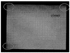
One of the primary quality control standards for MicroLED mura metrology involves high-resolution imaging systems. These systems utilize advanced cameras and image processing algorithms to capture and analyze the display output at a pixel-by-pixel level. The imaging process is typically conducted in a controlled environment with standardized lighting conditions to ensure accurate and repeatable measurements.
Another key standard in the quality control process is the use of spectroradiometers for precise color and luminance measurements. These instruments are calibrated to industry-standard color spaces, such as CIE 1931, to ensure accurate representation of color across the entire display. The measurements are taken at multiple points across the display surface to create a comprehensive map of color and brightness variations.
Statistical analysis methods form an integral part of the quality control standards for MicroLED displays. These methods involve the calculation of various metrics, such as standard deviation, uniformity, and contrast ratios, to quantify the extent of mura effects. Tolerance levels are established for each of these metrics, and displays that fall outside these tolerances are flagged for further investigation or correction.
Calibration workflows are standardized to ensure consistency across production lines. These workflows typically involve a multi-step process, including initial characterization, correction factor calculation, and verification. The calibration process aims to compensate for inherent variations in individual MicroLED elements, bringing the overall display output within specified uniformity tolerances.
Automated optical inspection (AOI) systems are increasingly becoming a standard in MicroLED quality control. These systems use machine vision and artificial intelligence algorithms to rapidly detect defects, including mura patterns, dead pixels, and color inconsistencies. AOI systems can process large volumes of displays in a production environment, significantly improving throughput and reliability compared to manual inspection methods.
To address the challenges of scaling quality control for large MicroLED displays, modular testing approaches have been developed. These standards involve testing individual modules or tiles before final assembly, allowing for early detection and correction of uniformity issues. This modular approach also facilitates more efficient replacement of defective components in the field.
Unlock deeper insights with Patsnap Eureka Quick Research — get a full tech report to explore trends and direct your research. Try now!
Generate Your Research Report Instantly with AI Agent
Supercharge your innovation with Patsnap Eureka AI Agent Platform!