MicroLED pixel uniformity tuning with active matrix compensation algorithms
AUG 21, 20259 MIN READ
Generate Your Research Report Instantly with AI Agent
Patsnap Eureka helps you evaluate technical feasibility & market potential.
MicroLED Background and Objectives
MicroLED technology has emerged as a promising next-generation display technology, offering significant advantages over traditional LED and OLED displays. The development of MicroLED displays can be traced back to the early 2000s, with pioneering work conducted by research institutions and technology companies. Over the past two decades, MicroLED has evolved from a concept to a viable technology with potential applications in various fields, including consumer electronics, automotive displays, and augmented reality devices.
The primary objective of MicroLED technology is to overcome the limitations of existing display technologies while offering superior performance characteristics. These include higher brightness, improved energy efficiency, longer lifespan, and better color reproduction. MicroLED displays aim to achieve these goals by utilizing arrays of microscopic LEDs, each serving as an individual pixel, allowing for precise control over light emission and color reproduction.
One of the critical challenges in MicroLED technology is achieving pixel uniformity across the entire display. This issue arises due to variations in the manufacturing process, which can lead to inconsistencies in the brightness and color output of individual MicroLED pixels. The non-uniformity can result in visible artifacts and reduced overall display quality, hindering the widespread adoption of MicroLED technology in commercial applications.
To address this challenge, researchers and engineers have been focusing on developing active matrix compensation algorithms. These algorithms aim to dynamically adjust the electrical characteristics of each MicroLED pixel to compensate for manufacturing variations and ensure uniform brightness and color across the entire display. The development of these compensation techniques is crucial for realizing the full potential of MicroLED technology and enabling its integration into various display applications.
The evolution of MicroLED technology is closely tied to advancements in semiconductor manufacturing processes, materials science, and display driver technologies. As the industry continues to invest in research and development, the goal is to overcome current technical hurdles and scale up production to make MicroLED displays commercially viable for a wide range of applications.
Looking ahead, the objectives for MicroLED technology include further miniaturization of LED elements, improved manufacturing yields, and the development of more sophisticated compensation algorithms. These advancements will be essential for enabling high-resolution, large-scale displays with exceptional image quality and uniformity. Additionally, researchers are exploring ways to integrate MicroLED technology with flexible substrates, opening up new possibilities for curved and foldable displays in the future.
Market Analysis for MicroLED Displays
The MicroLED display market is experiencing rapid growth and attracting significant attention from both industry players and consumers. This emerging technology offers several advantages over traditional display technologies, including higher brightness, better energy efficiency, and improved color accuracy. As a result, the demand for MicroLED displays is expected to increase substantially in the coming years across various sectors.
The consumer electronics segment, particularly smartphones and smartwatches, is anticipated to be a major driver of MicroLED adoption. These devices require high-resolution, energy-efficient displays that can operate in diverse lighting conditions. MicroLED technology's ability to deliver superior brightness and contrast ratios makes it an attractive option for manufacturers looking to differentiate their products in a competitive market.
The automotive industry is another key sector showing growing interest in MicroLED displays. As vehicles become more technologically advanced and incorporate larger infotainment systems, the demand for high-quality, durable displays is increasing. MicroLED's resistance to burn-in and long lifespan make it well-suited for automotive applications, where displays must withstand harsh environmental conditions and extended use.
In the television and large display market, MicroLED is positioned as a premium alternative to OLED and LCD technologies. While currently limited by high production costs, ongoing research and development efforts are focused on reducing manufacturing expenses and improving yield rates. As these challenges are addressed, MicroLED TVs are expected to gain market share in the high-end consumer segment.
The commercial and industrial sectors also present significant opportunities for MicroLED displays. Digital signage, control room displays, and large-scale visualization systems can benefit from MicroLED's high brightness, wide color gamut, and modular nature. These attributes allow for the creation of seamless, large-format displays that can operate in various lighting conditions and environments.
However, the widespread adoption of MicroLED technology faces several challenges. The most significant barrier is the high production cost, which currently limits its application to premium products. Additionally, the complexity of manufacturing processes, particularly in achieving uniform pixel performance across large arrays, presents technical hurdles that must be overcome to enable mass production.
Despite these challenges, the market outlook for MicroLED displays remains positive. Industry analysts project substantial growth in the coming years, driven by advancements in manufacturing techniques, increasing demand for high-performance displays, and the technology's potential to offer unique features in various applications. As research continues to address current limitations, particularly in areas such as pixel uniformity tuning and active matrix compensation algorithms, the MicroLED market is poised for expansion across multiple industries.
Technical Challenges in MicroLED Uniformity
MicroLED displays face significant challenges in achieving uniform pixel performance across large arrays. The primary technical hurdle lies in the inherent variability of individual LED elements, which can lead to noticeable differences in brightness and color among pixels. This non-uniformity stems from several factors, including variations in the manufacturing process, differences in electrical characteristics, and degradation over time.
One of the most pressing issues is the inconsistency in the current-voltage (I-V) characteristics of individual MicroLEDs. Even minor variations can result in substantial differences in light output, affecting the overall image quality. This challenge is exacerbated by the sheer number of pixels in a typical MicroLED display, where millions of individual LEDs must operate in harmony to produce a cohesive image.
Another significant obstacle is the color variation between pixels. MicroLEDs, especially those producing different colors (red, green, and blue), can exhibit disparities in their emission spectra and efficiency. This variation can lead to color inconsistencies across the display, compromising the accuracy and uniformity of the rendered image.
The miniaturization of LEDs to micro-scale dimensions introduces additional complexities. As the size of individual LEDs decreases, the impact of defects and edge effects becomes more pronounced. These factors can contribute to non-uniform current distribution within each MicroLED, further exacerbating the uniformity problem.
Temperature variations across the display panel present another challenge. MicroLEDs are sensitive to temperature changes, which can affect their performance and lifespan. Uneven heat distribution can lead to localized differences in brightness and color, particularly in large displays or those operating at high brightness levels.
Long-term stability and aging effects also pose significant challenges to maintaining uniformity over the lifespan of the display. MicroLEDs may degrade at different rates, leading to increasing non-uniformity over time. This degradation can be influenced by factors such as operating conditions, manufacturing variations, and the specific materials used in the LED structure.
Addressing these uniformity challenges requires sophisticated compensation techniques. Active matrix compensation algorithms play a crucial role in mitigating these issues by dynamically adjusting the drive signals for individual pixels. However, implementing these algorithms effectively presents its own set of challenges, including the need for high-resolution sensing and precise control circuitry integrated into the display backplane.
Current Uniformity Tuning Solutions
01 Pixel structure optimization
Improving the structure of individual MicroLED pixels to enhance uniformity. This may involve optimizing the shape, size, and arrangement of the LED elements within each pixel to ensure consistent light output across the display.- Pixel structure optimization: Improving the structure of individual MicroLED pixels to enhance uniformity. This includes optimizing the size, shape, and arrangement of the LED elements within each pixel to ensure consistent light output across the display. Advanced manufacturing techniques and materials are employed to achieve precise pixel structures.
- Driving circuit design: Developing sophisticated driving circuits to control MicroLED pixels uniformly. These circuits compensate for variations in individual LED characteristics, ensuring consistent current flow and brightness across all pixels. Advanced algorithms and feedback mechanisms are implemented to maintain uniformity over time and under different operating conditions.
- Color calibration techniques: Implementing advanced color calibration methods to achieve uniform color reproduction across MicroLED displays. This involves precise control of each subpixel's color output, compensating for manufacturing variations and aging effects. Spectral analysis and real-time adjustment algorithms are used to maintain color consistency.
- Defect detection and compensation: Developing systems for detecting and compensating for pixel defects in MicroLED displays. This includes in-line inspection during manufacturing and real-time monitoring during operation. Advanced image processing algorithms are used to identify non-uniform pixels and apply corrective measures, such as adjusting neighboring pixels to maintain overall uniformity.
- Thermal management for uniformity: Implementing effective thermal management solutions to maintain uniform pixel performance across MicroLED displays. This involves designing heat dissipation structures and using materials with optimal thermal properties. Temperature sensors and adaptive control systems are employed to ensure consistent operating temperatures, preventing thermal-induced variations in pixel brightness and color.
02 Driving circuit design
Developing advanced driving circuits to compensate for variations in MicroLED performance. These circuits can adjust the current or voltage supplied to each pixel, ensuring uniform brightness and color across the display.Expand Specific Solutions03 Manufacturing process control
Implementing precise control over the manufacturing process to minimize variations in MicroLED characteristics. This includes optimizing epitaxial growth, transfer processes, and bonding techniques to ensure consistent pixel performance.Expand Specific Solutions04 Calibration and compensation techniques
Developing advanced calibration and compensation algorithms to address non-uniformities in MicroLED displays. These techniques can involve measuring and adjusting individual pixel characteristics during production or in real-time during operation.Expand Specific Solutions05 Material and packaging innovations
Exploring new materials and packaging methods to improve MicroLED uniformity. This may include developing novel semiconductor materials, optimizing quantum well structures, or implementing advanced encapsulation techniques to protect MicroLEDs from environmental factors that could affect uniformity.Expand Specific Solutions
Key Players in MicroLED Industry
The MicroLED pixel uniformity tuning market is in its early growth stage, characterized by rapid technological advancements and increasing adoption in high-end display applications. The market size is expanding, driven by demand for superior image quality in premium devices. Technologically, the field is evolving quickly, with companies like IGNIS Innovation, BOE Technology, and Apple leading innovation. These firms are developing advanced active matrix compensation algorithms to address pixel uniformity challenges. Other key players such as Sharp, Innolux, and Samsung Electro-Mechanics are also contributing to the technological maturity of MicroLED displays, focusing on improving manufacturing processes and enhancing overall display performance.
IGNIS Innovation, Inc.
Technical Solution: IGNIS Innovation has developed advanced active matrix compensation algorithms for MicroLED pixel uniformity tuning. Their technology utilizes a combination of in-pixel sensing and external calibration to address non-uniformity issues in MicroLED displays. The company's MaxLife™ compensation technology employs real-time pixel-by-pixel correction to mitigate brightness and color variations across the display[1]. This system continuously monitors and adjusts each pixel's performance, ensuring consistent image quality over time. IGNIS's approach also incorporates machine learning algorithms to predict and preemptively correct potential uniformity issues, reducing the need for frequent recalibration[2].
Strengths: Real-time pixel-level compensation, predictive maintenance capabilities, and adaptability to various MicroLED configurations. Weaknesses: May require additional computational resources and potentially increase overall system complexity.
BOE Technology Group Co., Ltd.
Technical Solution: BOE has developed a comprehensive active matrix compensation system for MicroLED displays, focusing on large-scale applications such as video walls and outdoor displays. Their technology utilizes a distributed compensation architecture, combining local processing units with centralized control systems. BOE's approach incorporates real-time environmental sensing to adjust pixel performance based on ambient conditions[9]. The company's algorithm employs adaptive gamma correction and color temperature adjustment to maintain consistent image quality across varying viewing conditions. Additionally, BOE has implemented advanced defect management techniques to mitigate the impact of pixel failures and ensure long-term display reliability[10].
Strengths: Optimized for large-scale displays; robust environmental adaptation capabilities. Weaknesses: May require significant hardware infrastructure for distributed processing; potential challenges in achieving uniform performance across very large display areas.
Core Algorithms for Active Matrix Compensation
Display Method, Device, Display Equipment, and Storage Medium
PatentPendingCN120299392A
Innovation
- By dividing multiple luminescent pixels in the display panel into multiple luminescent pixel groups, and controlling the movement of the pixel offset device according to the gray scale value and proportional coefficient of each display pixel, the light path of the luminescent pixel is changed to ensure that light rays are incident to the corresponding display position and improve display uniformity.
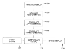
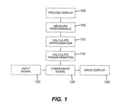
Method and apparatus for uniformity compensation in an electroluminescent display
PatentInactiveUS20080106491A1
Innovation
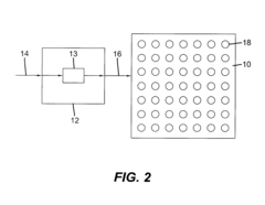
- A method that measures the performance of light-emitting elements at three or more different input intensity values to calculate parameters a and b, forming a linear transformation function to minimize errors and improve uniformity, reducing the complexity of calculations and storage requirements.
Manufacturing Process Optimization
Optimizing the manufacturing process for MicroLED displays with active matrix compensation algorithms is crucial for achieving pixel uniformity and enhancing overall display quality. The process begins with the careful selection and preparation of high-quality semiconductor materials, typically gallium nitride (GaN) or indium gallium nitride (InGaN), which form the basis of the MicroLED emitters.
The epitaxial growth of these materials requires precise control over temperature, pressure, and gas flow rates to ensure uniform crystal structure and composition. Advanced techniques such as metal-organic chemical vapor deposition (MOCVD) or molecular beam epitaxy (MBE) are employed to achieve the necessary precision. Following epitaxial growth, the wafer undergoes a series of photolithography and etching steps to define individual MicroLED pixels.
A critical aspect of the manufacturing process is the transfer and integration of MicroLED pixels onto the display backplane. Mass transfer techniques, such as pick-and-place or laser-assisted transfer, must be optimized to ensure accurate positioning and minimal damage to the delicate MicroLED structures. The integration of active matrix circuitry, including thin-film transistors (TFTs) for pixel addressing, is a complex process that requires careful alignment and bonding.
To address pixel uniformity issues, in-line testing and characterization techniques are implemented throughout the manufacturing process. These may include automated optical inspection systems, electrical testing, and spectral analysis to identify and map variations in brightness, color, and electrical characteristics across the display panel.
The incorporation of active matrix compensation algorithms into the manufacturing process involves the calibration and programming of individual pixel circuits. This step requires sophisticated testing equipment capable of measuring the performance of each MicroLED pixel and adjusting the driving parameters accordingly. The algorithms are designed to compensate for inherent variations in pixel characteristics, ensuring uniform brightness and color across the entire display.
Advanced process control systems are implemented to monitor and adjust manufacturing parameters in real-time. These systems utilize machine learning and artificial intelligence to analyze process data and make predictive adjustments, minimizing variations and improving yield. Continuous improvement methodologies, such as Six Sigma and statistical process control, are applied to identify and eliminate sources of variability in the manufacturing process.
By optimizing each stage of the manufacturing process and integrating active matrix compensation algorithms, manufacturers can significantly improve the uniformity and quality of MicroLED displays. This holistic approach to process optimization is essential for the successful commercialization of MicroLED technology and its adoption in high-end display applications.
Power Efficiency Considerations
Power efficiency is a critical consideration in the development and implementation of MicroLED displays, particularly when employing active matrix compensation algorithms for pixel uniformity tuning. The power consumption of MicroLED displays is directly influenced by the driving current required for each pixel, which in turn affects the overall energy efficiency of the device.
Active matrix compensation algorithms play a crucial role in optimizing power efficiency while maintaining pixel uniformity. These algorithms dynamically adjust the driving current for individual pixels, compensating for variations in brightness and color. By precisely controlling the current supplied to each MicroLED, the algorithms can minimize unnecessary power consumption without compromising display quality.
One of the key challenges in power efficiency optimization is balancing the trade-off between uniformity correction and energy consumption. Aggressive compensation algorithms may achieve better uniformity but at the cost of increased power usage. Therefore, it is essential to develop intelligent algorithms that can adapt to different display content and ambient lighting conditions, adjusting the compensation level accordingly.
The choice of driving circuitry also significantly impacts power efficiency. Advanced thin-film transistor (TFT) backplanes with low leakage currents and high electron mobility can reduce power losses in the active matrix. Additionally, implementing pulse-width modulation (PWM) techniques for driving MicroLEDs can further enhance power efficiency by allowing for precise control of pixel brightness through duty cycle adjustment rather than continuous current variation.
Thermal management is another crucial aspect of power efficiency in MicroLED displays. Efficient heat dissipation not only prolongs the lifespan of the display but also contributes to better power efficiency. As MicroLEDs generate less heat compared to traditional LED technologies, the cooling requirements are reduced, leading to potential energy savings in the overall system.
Furthermore, the development of low-power compensation algorithms that can operate in sleep or standby modes can significantly reduce the idle power consumption of MicroLED displays. These algorithms can maintain minimal uniformity correction during periods of inactivity, rapidly transitioning to full compensation when the display becomes active.
In conclusion, achieving optimal power efficiency in MicroLED displays with active matrix compensation algorithms requires a multifaceted approach. This includes developing sophisticated compensation algorithms, employing advanced driving circuitry, implementing effective thermal management strategies, and optimizing power consumption during idle states. As the technology continues to evolve, further improvements in power efficiency are expected, making MicroLED displays an increasingly attractive option for a wide range of applications.
Unlock deeper insights with Patsnap Eureka Quick Research — get a full tech report to explore trends and direct your research. Try now!
Generate Your Research Report Instantly with AI Agent
Supercharge your innovation with Patsnap Eureka AI Agent Platform!