MicroLED sidewall passivation methods to reduce efficiency loss in sub-10 μm pixels
AUG 21, 20259 MIN READ
Generate Your Research Report Instantly with AI Agent
Patsnap Eureka helps you evaluate technical feasibility & market potential.
MicroLED Passivation Background and Objectives
MicroLED technology has emerged as a promising candidate for next-generation displays, offering superior brightness, contrast, and energy efficiency compared to traditional LED and OLED technologies. The development of MicroLED displays has been driven by the increasing demand for high-performance, compact displays in various applications, including smartphones, smartwatches, augmented reality (AR), and virtual reality (VR) devices.
The evolution of MicroLED technology can be traced back to the early 2000s, with significant advancements made in the past decade. As the industry pushes towards higher resolution and smaller form factors, the need for sub-10 μm pixels has become increasingly critical. However, as pixel sizes decrease, efficiency loss due to sidewall defects becomes a major challenge, necessitating effective passivation methods.
Sidewall passivation is a crucial process in MicroLED fabrication, aimed at reducing non-radiative recombination centers and improving overall device performance. The primary objective of this research is to explore and evaluate various passivation techniques specifically tailored for sub-10 μm MicroLED pixels, with the goal of minimizing efficiency loss and enhancing device performance.
The technical goals of this research include:
1. Identifying and analyzing existing passivation methods applicable to MicroLED sidewalls.
2. Evaluating the effectiveness of different passivation techniques in reducing efficiency loss for sub-10 μm pixels.
3. Investigating novel passivation approaches that address the unique challenges posed by ultra-small pixel sizes.
4. Assessing the scalability and manufacturability of promising passivation methods for large-scale production.
This research is driven by the growing market demand for high-resolution, energy-efficient displays in consumer electronics and emerging technologies. The successful development of effective passivation methods for sub-10 μm MicroLED pixels will play a crucial role in advancing the technology towards commercialization and widespread adoption.
By addressing the efficiency loss issue in ultra-small pixels, this research aims to unlock the full potential of MicroLED technology, enabling the creation of displays with unprecedented pixel densities, improved color accuracy, and enhanced overall performance. The outcomes of this study will contribute significantly to the ongoing efforts to overcome the technical barriers in MicroLED manufacturing and pave the way for the next generation of display technologies.
Market Demand for High-Efficiency MicroLED Displays
The demand for high-efficiency MicroLED displays has been steadily increasing across various sectors, driven by the technology's superior performance characteristics and potential applications. The automotive industry, in particular, has shown significant interest in MicroLED displays for advanced driver assistance systems (ADAS) and in-vehicle infotainment systems. These displays offer enhanced brightness, contrast, and energy efficiency, making them ideal for use in challenging lighting conditions typical in automotive environments.
Consumer electronics represent another major market for MicroLED displays, with smartphones, smartwatches, and augmented reality (AR) devices leading the charge. The ability of MicroLED technology to deliver vibrant colors, high contrast ratios, and improved power efficiency aligns well with consumer demands for longer battery life and superior visual experiences. As the technology matures and production costs decrease, it is expected to penetrate deeper into the consumer electronics market, potentially replacing OLED in premium devices.
The professional display market, encompassing large-scale video walls, control room monitors, and high-end televisions, has also recognized the potential of MicroLED technology. The scalability of MicroLED displays allows for the creation of seamless, bezel-free screens of virtually any size, making them attractive for digital signage and luxury home entertainment systems. The long lifespan and resistance to burn-in further enhance their appeal in these applications.
In the medical field, there is a growing demand for high-resolution, high-contrast displays for diagnostic imaging. MicroLED technology's ability to provide precise color reproduction and high dynamic range makes it a promising candidate for next-generation medical monitors, potentially improving the accuracy of diagnoses and the efficiency of medical procedures.
The aerospace and defense sectors have shown interest in MicroLED displays for cockpit instrumentation and heads-up displays. The technology's high brightness and low power consumption are particularly valuable in these applications, where readability in varying light conditions and energy efficiency are critical.
As the push for more immersive virtual and augmented reality experiences continues, MicroLED displays are positioned to play a crucial role. Their ability to deliver high pixel densities, fast response times, and high brightness levels addresses many of the current limitations in VR and AR headsets, potentially opening up new markets and applications in gaming, training, and remote collaboration.
The overall market trajectory for high-efficiency MicroLED displays is expected to show substantial growth in the coming years. However, widespread adoption hinges on overcoming current technical challenges, including the development of efficient manufacturing processes for sub-10 μm pixels and effective sidewall passivation methods to reduce efficiency loss. As these hurdles are addressed, the market is likely to expand rapidly, with MicroLED technology potentially reshaping the display industry landscape.
Current Challenges in Sub-10 μm MicroLED Fabrication
The fabrication of sub-10 μm MicroLEDs presents several significant challenges that hinder the widespread adoption and commercialization of this promising technology. One of the primary issues is the increased surface-to-volume ratio as the pixel size decreases, which leads to a higher proportion of surface defects and non-radiative recombination centers. This phenomenon results in a substantial reduction in quantum efficiency and overall device performance.
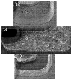
Another critical challenge is the difficulty in achieving uniform and precise etching of the sidewalls during the fabrication process. As the pixel size shrinks, the margin for error in etching becomes increasingly narrow, making it challenging to maintain consistent device characteristics across an array of MicroLEDs. Imperfections in the etching process can lead to rough sidewalls, which exacerbate the surface recombination problem and further decrease efficiency.
The passivation of MicroLED sidewalls becomes increasingly complex and crucial in sub-10 μm devices. Traditional passivation techniques that work well for larger LEDs may not be as effective at this scale due to the limited space and the need for ultra-thin, uniform coatings. The development of new passivation materials and methods that can effectively reduce surface states and prevent carrier leakage in such small structures is a significant challenge.
Moreover, the heat dissipation in sub-10 μm MicroLEDs poses a considerable problem. As the pixel size decreases, the current density increases, leading to localized heating that can affect the device's performance and lifespan. Efficient heat management strategies become critical but are challenging to implement in such confined spaces without compromising the optical properties of the device.
The integration of sub-10 μm MicroLEDs into display systems presents additional challenges. The precise placement and bonding of these tiny devices onto a backplane with high yield and accuracy require advanced pick-and-place technologies that are still in development. Furthermore, ensuring uniform current distribution and color consistency across an array of sub-10 μm MicroLEDs is a complex task that demands innovative driving schemes and compensation algorithms.
Lastly, the mass production of sub-10 μm MicroLEDs faces significant hurdles in terms of yield and cost-effectiveness. The stringent requirements for material quality, process control, and defect management at this scale make it challenging to achieve high yields in manufacturing. Overcoming these challenges to enable cost-effective, large-scale production of sub-10 μm MicroLEDs is crucial for their commercial viability in various applications, including next-generation displays and augmented reality devices.
Existing Sidewall Passivation Methods for MicroLEDs
01 Improving light extraction efficiency
Various techniques are employed to enhance the light extraction efficiency of MicroLEDs, reducing efficiency loss. These methods include optimizing the LED structure, using advanced materials, and implementing novel light extraction techniques to minimize internal reflection and maximize the amount of light emitted from the device.- Improving light extraction efficiency: Various techniques are employed to enhance the light extraction efficiency of MicroLEDs, reducing efficiency loss. These methods include optimizing the LED structure, implementing surface texturing, and using advanced packaging techniques to minimize light trapping within the device.
- Thermal management solutions: Effective thermal management is crucial for maintaining MicroLED efficiency. Innovative heat dissipation methods and materials are utilized to prevent efficiency loss due to temperature-related issues, ensuring optimal performance and longevity of the devices.
- Addressing current crowding: Current crowding in MicroLEDs can lead to significant efficiency loss. Advanced current spreading layers and electrode designs are implemented to ensure uniform current distribution across the device, thereby improving overall efficiency and reducing hotspots.
- Quantum efficiency enhancement: Techniques to improve the internal quantum efficiency of MicroLEDs are developed to minimize efficiency loss. These include optimizing the active region design, implementing quantum well structures, and using advanced materials to enhance carrier confinement and radiative recombination.
- Defect reduction strategies: Minimizing defects in MicroLED structures is essential for reducing efficiency loss. Advanced epitaxial growth techniques, substrate engineering, and post-growth treatments are employed to decrease crystal defects and improve the overall quality of MicroLED devices.
02 Thermal management solutions
Effective thermal management is crucial for maintaining MicroLED efficiency. Innovative heat dissipation methods and materials are developed to prevent efficiency loss due to overheating. These solutions aim to maintain optimal operating temperatures and extend the lifespan of MicroLED devices.Expand Specific Solutions03 Addressing current crowding
Current crowding in MicroLEDs can lead to efficiency loss and non-uniform light emission. Advanced electrode designs and current spreading layers are implemented to ensure uniform current distribution across the device, improving overall efficiency and light output uniformity.Expand Specific Solutions04 Optimizing quantum well structures
The design and optimization of quantum well structures in MicroLEDs play a crucial role in minimizing efficiency droop. Novel approaches to quantum well engineering, including the use of multiple quantum wells and barrier layers, are explored to enhance carrier confinement and reduce efficiency loss at high current densities.Expand Specific Solutions05 Defect reduction techniques
Minimizing defects in MicroLED structures is essential for reducing efficiency loss. Advanced growth techniques, substrate treatments, and post-growth processes are developed to reduce crystal defects, dislocations, and impurities that can act as non-radiative recombination centers and decrease overall device efficiency.Expand Specific Solutions
Key Players in MicroLED Industry and Research
The MicroLED sidewall passivation technology for sub-10 μm pixels is in an early development stage, with significant potential for growth as display technologies advance. The market size is expanding rapidly, driven by increasing demand for high-resolution, energy-efficient displays in various applications. While the technology is still maturing, several key players are making notable progress. Companies like Jade Bird Display, Apple, and Samsung Display are investing heavily in research and development to overcome efficiency challenges. Universities such as Xiamen University and Nanchang University are contributing valuable research. Established semiconductor firms like Applied Materials and Lumileds are leveraging their expertise to develop innovative solutions. The competitive landscape is diverse, with both startups and major corporations vying for technological breakthroughs in this promising field.
Canon, Inc.
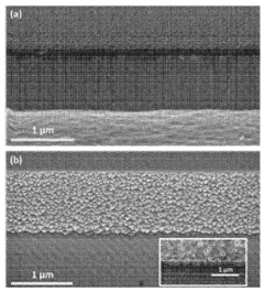
Technical Solution: Canon's approach to MicroLED sidewall passivation for sub-10 μm pixels focuses on a high-temperature, all-inorganic solution. They employ a two-step process starting with a high-temperature (800-1000°C) thermal oxidation to create a thin SiO2 layer directly on the LED sidewalls [7]. This is followed by the deposition of a silicon oxynitride (SiOxNy) layer using high-density plasma chemical vapor deposition (HDP-CVD) at temperatures around 300-400°C [8]. The SiOxNy layer composition is carefully controlled to optimize stress and refractive index. Canon has also developed a proprietary annealing process that uses rapid thermal annealing (RTA) with a specific temperature profile to reduce interface states and improve passivation quality [9].
Strengths: High-temperature process creates a dense, high-quality passivation layer with excellent stability. The graded composition of SiOxNy allows for stress management and refractive index optimization. Weaknesses: High-temperature steps may limit compatibility with certain substrate materials and increase thermal budget.
Applied Materials, Inc.
Technical Solution: Applied Materials has developed a comprehensive MicroLED sidewall passivation solution for sub-10 μm pixels using their advanced deposition and treatment equipment. Their method involves a multi-layer approach starting with a thin AlN buffer layer deposited by reactive sputtering, typically 5-10 nm thick [10]. This is followed by alternating layers of Al2O3 and HfO2 deposited by atomic layer deposition (ALD), with each layer being 2-5 nm thick [11]. The total passivation stack is usually 20-40 nm thick. Applied Materials has also integrated an in-situ plasma treatment step between layer depositions to enhance interface quality. Additionally, they have developed a post-deposition annealing process using their rapid thermal processing (RTP) equipment, which incorporates a controlled ambient of N2 and H2 to passivate dangling bonds and reduce interface traps [12].
Strengths: Highly conformal and pinhole-free passivation layers due to ALD. The multi-layer approach allows for stress management and optimization of optical properties. In-situ plasma treatment and post-deposition annealing improve interface quality. Weaknesses: The complex multi-layer structure and additional treatment steps may increase production time and cost.
Core Innovations in Sub-10 μm MicroLED Passivation
Micro-leds with ultra-low leakage current
PatentPendingKR1020240107341A
Innovation
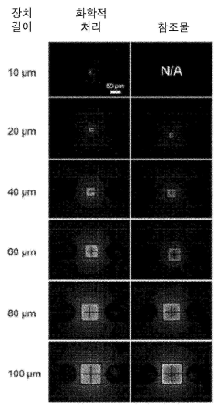
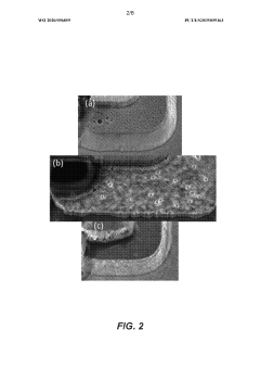
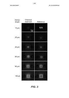
- A manufacturing method involving chemical treatment followed by conformal dielectric deposition, specifically using potassium hydroxide (KOH) treatment and atomic layer deposition (ALD) sidewall passivation, to remove sidewall damage and reduce leakage current, resulting in uniform light emission and improved efficiency.

Micro-LEDS with ultra-low leakage current
PatentWO2020096859A1
Innovation
- A combination of chemical treatment and conformal dielectric sidewall passivation, specifically using potassium hydroxide (KOH) chemical treatment followed by atomic-layer deposition (ALD) sidewall passivation, to remove sidewall damage and surface states, thereby reducing leakage current and enhancing the efficiency of micro-LEDs.

Material Considerations for Effective Passivation
The selection of appropriate materials for effective passivation is crucial in reducing efficiency loss in sub-10 μm MicroLED pixels. The primary goal of passivation is to minimize surface recombination and protect the sidewalls from environmental degradation. To achieve this, several material properties must be considered.
Firstly, the passivation material should have a wide bandgap to create a potential barrier that prevents carriers from reaching the surface. Materials such as silicon dioxide (SiO2) and aluminum oxide (Al2O3) are commonly used due to their excellent insulating properties and compatibility with semiconductor processing.
Chemical stability is another critical factor. The passivation layer must withstand the harsh conditions during device fabrication and operation. Materials like silicon nitride (Si3N4) offer superior chemical resistance and serve as an effective diffusion barrier against impurities.
The thermal expansion coefficient of the passivation material should closely match that of the MicroLED structure to minimize stress at the interface. This is particularly important for sub-10 μm pixels, where even small mismatches can lead to significant strain and potential device failure.
Optical properties of the passivation layer play a vital role in light extraction efficiency. Materials with high refractive indices, such as titanium dioxide (TiO2), can enhance light output by reducing total internal reflection. However, the trade-off between passivation quality and optical performance must be carefully balanced.
Deposition method compatibility is essential for achieving conformal coverage on the high-aspect-ratio sidewalls of sub-10 μm MicroLEDs. Atomic Layer Deposition (ALD) is often preferred for its ability to produce uniform, pinhole-free films with precise thickness control.
The interface quality between the passivation layer and the MicroLED material is critical. Materials that can form a high-quality interface with minimal defects and dangling bonds are ideal. Surface treatments and interface engineering techniques may be employed to optimize this aspect.
Lastly, the long-term stability of the passivation material under various operating conditions must be considered. Resistance to moisture, temperature cycling, and electrical stress are essential for ensuring the longevity of MicroLED devices in diverse applications.
Environmental Impact of MicroLED Manufacturing Processes
The environmental impact of MicroLED manufacturing processes is a critical consideration as this technology gains prominence in the display industry. The production of MicroLEDs, particularly those with sub-10 μm pixels, involves complex fabrication steps that can have significant environmental implications.
One of the primary environmental concerns is the use of rare earth elements in MicroLED production. These materials, essential for creating the light-emitting components, often require extensive mining operations that can lead to habitat destruction and soil contamination. The extraction process also consumes substantial energy, contributing to increased carbon emissions.
Chemical processes involved in MicroLED manufacturing, including etching and deposition, utilize various hazardous substances. These chemicals, if not properly managed, can pose risks to local ecosystems and water sources. Proper disposal and treatment of these materials are crucial to mitigate environmental damage.
The fabrication of MicroLEDs demands stringent cleanroom conditions, necessitating high energy consumption for maintaining controlled environments. This energy-intensive process contributes to the overall carbon footprint of MicroLED production. Additionally, the need for precise temperature control and specialized equipment further increases energy requirements.
Water usage is another significant environmental factor in MicroLED manufacturing. The production process requires large volumes of ultra-pure water for cleaning and processing, potentially straining local water resources. Efficient water recycling systems are essential to reduce the environmental impact of this water-intensive industry.
The miniaturization of MicroLEDs to sub-10 μm pixels introduces additional environmental challenges. The increased precision required in manufacturing these smaller pixels often leads to higher defect rates, resulting in more waste material. Developing more efficient production techniques and improving yield rates are crucial for minimizing this waste.
As the industry moves towards mass production of MicroLEDs, the cumulative environmental impact becomes more pronounced. Scaling up production while maintaining environmental sustainability presents a significant challenge. Innovations in manufacturing processes, such as more efficient passivation methods, can play a crucial role in reducing the overall environmental footprint of MicroLED technology.
Unlock deeper insights with Patsnap Eureka Quick Research — get a full tech report to explore trends and direct your research. Try now!
Generate Your Research Report Instantly with AI Agent
Supercharge your innovation with Patsnap Eureka AI Agent Platform!