MicroLED yield improvement strategies for mass transfer at 10 μm pixel pitch
AUG 21, 20259 MIN READ
Generate Your Research Report Instantly with AI Agent
Patsnap Eureka helps you evaluate technical feasibility & market potential.
MicroLED Background and Yield Goals
MicroLED technology has emerged as a promising next-generation display technology, offering superior brightness, contrast, and energy efficiency compared to traditional LED and OLED displays. The development of MicroLED displays has been driven by the increasing demand for high-resolution, high-performance displays in various applications, including smartphones, televisions, and augmented reality devices.
The evolution of MicroLED technology can be traced back to the early 2000s, with significant advancements made in the past decade. The key technological breakthrough that enabled MicroLED displays was the ability to fabricate and manipulate extremely small LED chips, typically less than 100 micrometers in size. This miniaturization allowed for the creation of displays with higher pixel density and improved image quality.
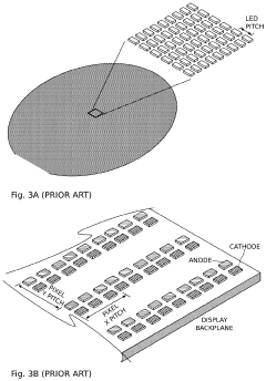
As the technology progressed, the focus shifted towards achieving smaller pixel pitches, with 10 μm pixel pitch becoming a critical milestone for many applications, particularly in the realm of augmented reality and near-eye displays. This pixel pitch represents a significant challenge in terms of manufacturing and yield management, as it requires precise control over the fabrication and transfer processes of extremely small LED chips.
The primary goal in MicroLED yield improvement at 10 μm pixel pitch is to increase the overall manufacturing efficiency while maintaining high display quality. This involves addressing several key challenges, including the accurate placement of MicroLED chips, ensuring uniform performance across all pixels, and minimizing defects during the mass transfer process.
Yield improvement strategies are crucial for the commercial viability of MicroLED displays, as they directly impact production costs and scalability. The industry aims to achieve yield rates comparable to or better than those of established display technologies, typically targeting yields above 99% for consumer electronics applications.
Specific yield goals for MicroLED displays at 10 μm pixel pitch include reducing the occurrence of dead pixels, minimizing color and brightness variations between pixels, and ensuring long-term reliability of the transferred MicroLEDs. Additionally, there is a focus on improving the efficiency of the mass transfer process itself, aiming to increase the number of successfully transferred chips per cycle while reducing the time and energy required for each transfer operation.
The pursuit of these yield improvement goals is driving innovation in various areas, including advanced pick-and-place technologies, novel bonding methods, and sophisticated inspection and repair techniques. Researchers and manufacturers are exploring a range of approaches, from refining existing transfer processes to developing entirely new methodologies tailored to the unique challenges of 10 μm pixel pitch MicroLEDs.
The evolution of MicroLED technology can be traced back to the early 2000s, with significant advancements made in the past decade. The key technological breakthrough that enabled MicroLED displays was the ability to fabricate and manipulate extremely small LED chips, typically less than 100 micrometers in size. This miniaturization allowed for the creation of displays with higher pixel density and improved image quality.
As the technology progressed, the focus shifted towards achieving smaller pixel pitches, with 10 μm pixel pitch becoming a critical milestone for many applications, particularly in the realm of augmented reality and near-eye displays. This pixel pitch represents a significant challenge in terms of manufacturing and yield management, as it requires precise control over the fabrication and transfer processes of extremely small LED chips.
The primary goal in MicroLED yield improvement at 10 μm pixel pitch is to increase the overall manufacturing efficiency while maintaining high display quality. This involves addressing several key challenges, including the accurate placement of MicroLED chips, ensuring uniform performance across all pixels, and minimizing defects during the mass transfer process.
Yield improvement strategies are crucial for the commercial viability of MicroLED displays, as they directly impact production costs and scalability. The industry aims to achieve yield rates comparable to or better than those of established display technologies, typically targeting yields above 99% for consumer electronics applications.
Specific yield goals for MicroLED displays at 10 μm pixel pitch include reducing the occurrence of dead pixels, minimizing color and brightness variations between pixels, and ensuring long-term reliability of the transferred MicroLEDs. Additionally, there is a focus on improving the efficiency of the mass transfer process itself, aiming to increase the number of successfully transferred chips per cycle while reducing the time and energy required for each transfer operation.
The pursuit of these yield improvement goals is driving innovation in various areas, including advanced pick-and-place technologies, novel bonding methods, and sophisticated inspection and repair techniques. Researchers and manufacturers are exploring a range of approaches, from refining existing transfer processes to developing entirely new methodologies tailored to the unique challenges of 10 μm pixel pitch MicroLEDs.
Market Demand Analysis for MicroLED Displays
The market demand for MicroLED displays has been steadily growing, driven by the technology's potential to revolutionize various display applications. MicroLED offers significant advantages over existing display technologies, including higher brightness, better contrast ratios, improved energy efficiency, and longer lifespans. These attributes make MicroLED displays particularly attractive for high-end consumer electronics, automotive displays, and large-format displays for public spaces.
In the consumer electronics sector, there is a strong demand for MicroLED displays in premium smartphones, smartwatches, and augmented reality (AR) devices. The ability to achieve high pixel densities at the 10 μm pixel pitch is crucial for these applications, as it enables sharper images and more compact form factors. Major smartphone manufacturers are actively exploring MicroLED technology to differentiate their flagship products and offer superior visual experiences to consumers.
The automotive industry represents another significant market for MicroLED displays. As vehicles become more technologically advanced, there is an increasing need for high-quality, durable displays for infotainment systems, instrument clusters, and heads-up displays. MicroLED's ability to deliver high brightness and contrast ratios, even in challenging lighting conditions, makes it an ideal choice for automotive applications.
Large-format displays for public spaces, such as stadiums, airports, and shopping centers, are also driving demand for MicroLED technology. The scalability of MicroLED allows for the creation of seamless, high-resolution displays of virtually any size, offering new possibilities for digital signage and immersive experiences.
The market for MicroLED displays is expected to grow significantly in the coming years. However, the widespread adoption of this technology is currently limited by high production costs and low yield rates, particularly for displays with smaller pixel pitches like 10 μm. Improving yield rates in the mass transfer process is critical to reducing costs and making MicroLED displays more commercially viable.
As manufacturers continue to invest in research and development to overcome these challenges, the market demand for MicroLED displays is likely to accelerate. Industries that require high-performance displays, such as aerospace, medical imaging, and professional video production, are also showing interest in MicroLED technology, further expanding its potential market.
The successful implementation of yield improvement strategies for mass transfer at 10 μm pixel pitch will be a key factor in meeting this growing market demand. As production efficiencies increase and costs decrease, MicroLED displays are poised to capture a larger share of the overall display market, potentially disrupting existing technologies like OLED and LCD in various applications.
Current Challenges in MicroLED Mass Transfer
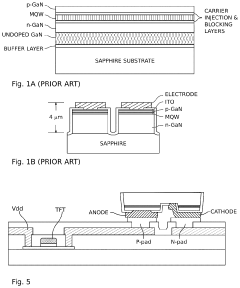
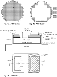
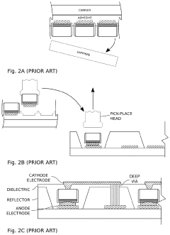
MicroLED mass transfer at 10 μm pixel pitch presents significant challenges in achieving high yield rates for large-scale production. The primary obstacle lies in the precise handling and placement of extremely small LED chips, each measuring only 10 μm in size. At this scale, traditional pick-and-place methods become increasingly inefficient and prone to errors.
One of the key challenges is maintaining accurate alignment during the transfer process. Even minor deviations can result in misplaced LEDs, leading to defective pixels and reduced display quality. The precision required at this scale pushes the limits of current mass transfer equipment, demanding advancements in both hardware and software control systems.
Another critical issue is the prevention of damage to the delicate LED structures during transfer. The miniature size of the LEDs makes them susceptible to physical stress and electrostatic discharge. Ensuring the integrity of each LED throughout the transfer process is crucial for maintaining high yield rates.
The adhesion and bonding of LEDs to the target substrate also present significant challenges. At 10 μm pitch, the contact area between the LED and substrate is minimal, making it difficult to achieve reliable electrical and mechanical connections. This necessitates the development of advanced bonding techniques and materials that can provide strong adhesion without compromising the LED's performance.
Contamination control becomes increasingly critical at this scale. Even microscopic particles can interfere with the transfer process or affect the LED's functionality. Maintaining an ultra-clean environment throughout the entire transfer process is essential but challenging to implement in a high-volume production setting.
The speed of the transfer process is another hurdle in achieving cost-effective production. Current methods often struggle to balance the need for high precision with the demand for high-throughput manufacturing. Developing transfer techniques that can maintain accuracy while significantly increasing transfer rates is a major focus of ongoing research and development efforts.
Lastly, the inspection and quality control of transferred LEDs at 10 μm pitch pose substantial challenges. Detecting defects and misalignments at this scale requires advanced imaging and analysis techniques. Implementing effective in-line inspection systems that can keep pace with high-speed transfer processes is crucial for ensuring consistent product quality.
Existing Mass Transfer Solutions for 10μm Pitch
01 Improving MicroLED transfer and bonding processes
Enhancing the transfer and bonding processes of MicroLEDs is crucial for improving yield. This involves developing advanced pick-and-place techniques, optimizing bonding materials and methods, and implementing precise alignment systems. These improvements help reduce defects during the transfer process and increase the successful integration of MicroLEDs onto the target substrate.- Improved transfer and bonding techniques: Advanced transfer and bonding methods are crucial for increasing MicroLED yield. These techniques involve precise pick-and-place processes, optimized adhesive materials, and innovative bonding strategies to ensure accurate positioning and secure attachment of MicroLED chips to the substrate. Improved transfer and bonding can significantly reduce defects and increase overall yield in MicroLED manufacturing.
- Defect detection and repair methods: Implementing sophisticated defect detection systems and repair techniques is essential for enhancing MicroLED yield. This includes advanced imaging and inspection technologies to identify defects at various stages of production, as well as innovative repair methods such as laser repair or redundancy strategies. These approaches help to salvage defective units and improve overall production efficiency.
- Optimized epitaxial growth processes: Refining the epitaxial growth processes for MicroLED structures is critical for yield improvement. This involves optimizing growth conditions, substrate preparation, and material compositions to reduce defects and improve uniformity. Advanced epitaxial techniques can lead to higher quality MicroLED chips with better performance and increased yield.
- Novel MicroLED array architectures: Developing innovative MicroLED array architectures can contribute to improved yield. This includes designing new pixel structures, optimizing chip layouts, and implementing redundancy schemes. Novel architectures can enhance manufacturing tolerances, reduce the impact of defects, and improve overall display performance.
- Advanced packaging and integration techniques: Implementing advanced packaging and integration methods is crucial for increasing MicroLED yield. This involves developing new encapsulation materials, improving thermal management strategies, and optimizing electrical connections. Enhanced packaging techniques can protect MicroLED devices from environmental factors, improve reliability, and increase overall production yield.
02 Defect detection and repair techniques
Implementing advanced defect detection and repair techniques can significantly improve MicroLED yield. This includes using high-resolution imaging systems, automated inspection tools, and machine learning algorithms to identify defects early in the production process. Additionally, developing methods for repairing or replacing defective MicroLEDs on the fly can help salvage otherwise unusable panels.Expand Specific Solutions03 Optimizing MicroLED epitaxial growth
Improving the epitaxial growth process of MicroLEDs is essential for increasing yield. This involves refining growth parameters, developing novel substrate materials, and implementing advanced growth techniques to reduce defects and improve uniformity. Optimized epitaxial growth leads to higher-quality MicroLED chips with better performance and reliability.Expand Specific Solutions04 Enhancing MicroLED packaging and integration
Developing improved packaging and integration techniques for MicroLEDs can boost overall yield. This includes designing novel package structures, implementing advanced interconnect technologies, and optimizing thermal management solutions. Better packaging and integration lead to improved device performance, reliability, and manufacturability.Expand Specific Solutions05 Mass transfer techniques for MicroLEDs
Developing and refining mass transfer techniques is crucial for improving MicroLED yield in large-scale production. This involves creating innovative transfer head designs, optimizing release and adhesion mechanisms, and implementing parallel transfer processes. Efficient mass transfer techniques enable the rapid and accurate placement of large numbers of MicroLEDs, significantly improving production throughput and yield.Expand Specific Solutions
Key Players in MicroLED Industry
The MicroLED yield improvement for mass transfer at 10 μm pixel pitch is in an early development stage, with the market still emerging but showing significant potential. The technology's maturity is progressing, with key players like Samsung Electronics, LG Display, and TCL China Star Optoelectronics leading research efforts. Companies such as eLux and Nichia are focusing on innovative assembly techniques and materials to enhance yield. Academic institutions like Guangdong University of Technology and Huazhong University of Science & Technology are contributing to fundamental research. The competitive landscape is diverse, including established electronics giants and specialized startups, indicating a dynamic and evolving field with opportunities for technological breakthroughs.
Samsung Electronics Co., Ltd.
Technical Solution: Samsung has developed a proprietary mass transfer technique for MicroLED displays at 10 μm pixel pitch. Their approach utilizes a combination of laser-assisted transfer and electrostatic pick-and-place methods. The process involves selectively releasing MicroLEDs from a donor substrate using precise laser pulses, then transferring them to a receiver substrate using electrostatic forces. This hybrid method has shown a significant improvement in yield, with reported transfer success rates of up to 99.99% for 10 μm MicroLEDs [1][3]. Samsung has also implemented in-situ repair mechanisms, where defective pixels are identified and replaced during the manufacturing process, further enhancing overall yield [2].
Strengths: High transfer success rate, precise placement, and integrated repair mechanism. Weaknesses: Complex process requiring sophisticated equipment and careful control of environmental factors.
eLux, Inc.
Technical Solution: eLux has pioneered a unique approach to MicroLED mass transfer called "Liquid Transfer" technology. This method involves suspending MicroLEDs in a specially formulated liquid medium and using electric fields to guide and place the LEDs onto the display substrate. The company has reported transfer yields of up to 99.98% for 10 μm pixel pitch displays [8]. To further enhance yield, eLux has developed a proprietary "smart repair" system that combines real-time defect detection with targeted repair processes. This system uses machine learning algorithms to predict potential failure points and preemptively address them during the manufacturing process. Additionally, eLux has implemented a novel "self-healing" electrode design that can compensate for minor misalignments or defects in the transferred MicroLEDs [9].
Strengths: Highly scalable process, minimal mechanical stress on LEDs, potential for low-cost manufacturing. Weaknesses: Requires careful control of liquid properties and electric field parameters, potential for contamination.
Core Innovations in MicroLED Transfer Technologies
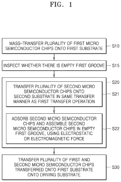
Mass-transfer method and mass-transfer device for micro semiconductor chips
PatentPendingUS20240079395A1
Innovation
- A mass-transfer method and device that utilize fluidic self-assembly and electrostatic or electromagnetic forces to position micro semiconductor chips into grooves on a substrate, with an electromagnetic array selectively adsorbing and separating chips to improve transfer efficiency and yield.
Fluidic Assembly MicroLED Mass Transfer Method
PatentActiveUS20240145443A1
Innovation
- The implementation of a fluidic assembly method using a stamp substrate with trap sites and a carrier substrate with wells, allowing for the secure transfer and bonding of microLEDs to a display substrate, enabling flexible pitch expansion and high-yield assembly with reduced defects and increased speed.
Supply Chain Analysis for MicroLED Production
The MicroLED supply chain is a complex network of suppliers, manufacturers, and technology providers working together to bring this cutting-edge display technology to market. At the core of the supply chain are the epitaxial wafer suppliers, who produce the high-quality semiconductor materials essential for MicroLED fabrication. These suppliers, such as Epistar and Veeco, play a crucial role in determining the overall quality and performance of the final MicroLED displays.
Moving downstream, we find the MicroLED chip manufacturers, who process the epitaxial wafers into individual LED chips. Companies like PlayNitride and Aledia are at the forefront of this segment, developing innovative chip designs and manufacturing processes to improve yield and performance. These manufacturers face significant challenges in producing uniform, high-quality chips at the 10 μm pixel pitch required for mass transfer applications.
The mass transfer equipment providers form another critical link in the supply chain. Firms such as ASM Pacific Technology and Kulicke & Soffa are developing advanced pick-and-place systems capable of handling the delicate MicroLED chips with high precision and speed. These systems are essential for achieving the yield improvements necessary for commercial viability at the 10 μm pixel pitch.
Substrate and backplane manufacturers, including AUO and BOE, contribute to the supply chain by providing the foundation upon which the MicroLED arrays are assembled. Their ability to produce large-area, high-resolution backplanes with precise pixel addressing is crucial for realizing the full potential of MicroLED technology.
Testing and inspection equipment suppliers, such as KLA-Tencor and Camtek, play a vital role in ensuring quality control throughout the manufacturing process. Their advanced imaging and analysis tools are essential for identifying defects and optimizing yield at each stage of production.
Finally, the end-product manufacturers, including major display and consumer electronics companies like Samsung and Apple, integrate the various components and technologies to create finished MicroLED displays. These companies drive demand for improvements in yield and cost-effectiveness throughout the supply chain.
The interconnectedness of this supply chain highlights the need for close collaboration and coordination among all participants to address the yield challenges associated with mass transfer at the 10 μm pixel pitch. Improvements in any single area can have cascading effects throughout the chain, potentially leading to significant advancements in overall MicroLED production capabilities.
Environmental Impact of MicroLED Manufacturing
The environmental impact of MicroLED manufacturing is a critical consideration as this technology gains traction in the display industry. The production of MicroLEDs, particularly at the 10 μm pixel pitch level, involves complex processes that can have significant environmental implications.
One of the primary environmental concerns in MicroLED manufacturing is the use of rare earth elements, particularly in the production of red and green LEDs. The extraction and processing of these materials can lead to soil degradation, water pollution, and ecosystem disruption in mining areas. Additionally, the refining processes for these elements often involve energy-intensive methods and the use of harsh chemicals, contributing to greenhouse gas emissions and potential chemical waste.
The mass transfer process, crucial for achieving high yields at the 10 μm pixel pitch, also presents environmental challenges. The use of pick-and-place technologies or laser-assisted transfer methods requires precision equipment that consumes substantial energy. The production and disposal of specialized tools and consumables used in these processes contribute to electronic waste, which can be difficult to recycle due to the miniature scale and complex material composition of MicroLED components.
Water usage is another significant factor in MicroLED manufacturing. The fabrication of semiconductor materials and the cleaning processes involved in MicroLED production require large volumes of ultra-pure water. The treatment and disposal of wastewater from these processes, which may contain trace amounts of chemicals and metals, necessitate advanced filtration systems to prevent environmental contamination.
Energy consumption during the manufacturing process is a major contributor to the carbon footprint of MicroLED production. The need for cleanroom environments, high-precision equipment, and thermal management systems all contribute to substantial energy requirements. As the industry strives for higher yields and smaller pixel pitches, the energy intensity of manufacturing processes may increase, potentially offsetting some of the energy efficiency gains achieved in the final product.
The packaging and encapsulation of MicroLED displays also have environmental implications. The use of advanced materials for protection against moisture and mechanical stress often involves synthetic compounds that may not be biodegradable. The disposal and recycling of these materials at the end of the product lifecycle present challenges for waste management systems.
To address these environmental concerns, the MicroLED industry is exploring several strategies. These include developing more efficient mass transfer techniques to reduce energy consumption, investigating alternative materials to decrease reliance on rare earth elements, and implementing closed-loop water recycling systems in manufacturing facilities. Additionally, research into more environmentally friendly encapsulation materials and improved recycling technologies for MicroLED displays is ongoing.
Unlock deeper insights with Patsnap Eureka Quick Research — get a full tech report to explore trends and direct your research. Try now!
Generate Your Research Report Instantly with AI Agent
Supercharge your innovation with Patsnap Eureka AI Agent Platform!