Patent Analysis of Innovations in Neuromorphic Materials
OCT 27, 20259 MIN READ
Generate Your Research Report Instantly with AI Agent
Patsnap Eureka helps you evaluate technical feasibility & market potential.
Neuromorphic Materials Innovation Background and Objectives
Neuromorphic computing represents a paradigm shift in computational architecture, drawing inspiration from the structure and function of biological neural systems. The evolution of this field has been marked by significant advancements in materials science, transitioning from traditional silicon-based components to novel neuromorphic materials capable of mimicking synaptic plasticity and neural dynamics. Since the concept's inception in the late 1980s by Carver Mead, the trajectory has moved from theoretical frameworks to practical implementations, with accelerated development observed in the past decade.
The fundamental goal of neuromorphic materials innovation is to overcome the limitations of von Neumann architecture by creating computing systems that integrate memory and processing functions, similar to biological neural networks. This approach aims to address the increasing energy consumption and performance bottlenecks in conventional computing systems, particularly for artificial intelligence applications that require massive parallel processing capabilities.
Recent technological advancements have expanded the scope of neuromorphic materials to include memristive devices, phase-change materials, spintronic components, and organic electronic materials. These innovations seek to replicate key neurobiological functions such as spike-timing-dependent plasticity (STDP), long-term potentiation (LTP), and long-term depression (LTD) at the material level, enabling more efficient and biologically realistic computational processes.
Patent analysis in this domain reveals a growing emphasis on materials that can facilitate adaptive learning, ultra-low power consumption, and fault tolerance. The innovation landscape has evolved from focusing primarily on device-level improvements to encompassing system-level architectures that leverage the unique properties of neuromorphic materials. This shift reflects the recognition that true neuromorphic computing requires holistic design approaches that consider both material properties and computational frameworks.
The technical objectives for neuromorphic materials development include achieving higher integration density, reducing energy consumption to sub-femtojoule per synaptic event, improving switching speed and reliability, and enhancing scalability for large-scale neural networks. Additionally, there is a growing focus on developing materials compatible with existing semiconductor manufacturing processes to facilitate commercial adoption.
As the field progresses, interdisciplinary collaboration between materials scientists, electrical engineers, computer scientists, and neuroscientists has become increasingly important. This convergence of expertise aims to bridge the gap between theoretical understanding of neural processes and practical implementation in material systems, ultimately working toward the creation of truly brain-inspired computing architectures that can revolutionize applications in pattern recognition, autonomous systems, and cognitive computing.
Market Demand Analysis for Neuromorphic Computing Solutions
The neuromorphic computing market is experiencing significant growth driven by increasing demand for AI applications that require more efficient processing capabilities. Current market projections indicate the global neuromorphic computing market will reach approximately $8.9 billion by 2025, with a compound annual growth rate of 49.1% from 2020. This remarkable growth trajectory reflects the expanding need for computing solutions that can process complex neural network operations while minimizing energy consumption.
The primary market demand stems from industries requiring advanced pattern recognition, real-time data processing, and autonomous decision-making capabilities. Healthcare represents a substantial segment, where neuromorphic systems enable faster medical image analysis, patient monitoring, and drug discovery processes. The automotive industry constitutes another significant market, with self-driving vehicles requiring neuromorphic processors for instantaneous environmental perception and navigation decisions.
Edge computing applications represent a rapidly expanding market segment for neuromorphic solutions. As IoT devices proliferate, the need for on-device intelligence that operates with minimal power consumption becomes increasingly critical. Market research indicates that approximately 75% of enterprise-generated data will be processed at the edge by 2025, creating substantial opportunities for neuromorphic computing implementations.
The defense and aerospace sectors demonstrate growing interest in neuromorphic materials and computing architectures. These industries require systems capable of operating in harsh environments while performing complex recognition tasks with minimal latency. Market analysis reveals defense applications alone could account for 18% of the neuromorphic computing market by 2026.
Energy efficiency represents a primary market driver, with data centers seeking solutions to reduce their substantial power consumption. Traditional computing architectures face fundamental limitations in energy efficiency when scaling to handle complex AI workloads. Market surveys indicate that 67% of enterprise technology decision-makers cite energy consumption as a critical factor when evaluating new computing infrastructure.
The academic and research sector constitutes a significant market segment, with universities and research institutions investing in neuromorphic computing platforms for advanced scientific applications. This segment serves as both a customer base and an innovation driver, creating a positive feedback loop for market expansion.
Geographic market distribution shows North America currently leading adoption with approximately 42% market share, followed by Europe at 28% and Asia-Pacific at 24%. However, the Asia-Pacific region demonstrates the fastest growth rate, driven by substantial investments in AI infrastructure by countries like China, Japan, and South Korea.
Current State and Challenges in Neuromorphic Materials Development
The field of neuromorphic materials has witnessed significant advancements globally, yet remains in a relatively nascent stage of development. Current research predominantly focuses on memristive materials, phase-change materials, and spintronic devices that can emulate synaptic and neuronal functions. Silicon-based neuromorphic chips from companies like Intel (Loihi) and IBM (TrueNorth) represent the most mature implementations, though they still face substantial limitations in energy efficiency and scalability compared to biological neural systems.
A primary challenge in neuromorphic materials development is achieving the perfect balance between stability and plasticity. Materials must maintain consistent performance over extended periods while simultaneously demonstrating the flexibility to adapt to new inputs—a fundamental property of biological neural networks that remains difficult to replicate in artificial systems. This stability-plasticity dilemma represents one of the field's most significant technical hurdles.
Energy efficiency presents another critical challenge. Despite improvements, current neuromorphic systems still consume orders of magnitude more energy per operation than their biological counterparts. The human brain operates at approximately 20 watts, while comparable artificial systems require substantially more power, limiting their practical deployment in edge computing and mobile applications where energy constraints are paramount.
Fabrication complexity and scalability issues further impede progress. Many promising neuromorphic materials demonstrate excellent properties in laboratory settings but face significant manufacturing challenges when scaled to commercial production. Integration with conventional CMOS technology presents particular difficulties, as novel materials often require specialized fabrication processes incompatible with established semiconductor manufacturing techniques.
Geographically, research leadership in neuromorphic materials is distributed across North America, Europe, and East Asia. The United States leads in fundamental research and commercialization efforts through companies like Intel and IBM, alongside academic powerhouses such as MIT and Stanford. Europe demonstrates strength in materials science innovation, particularly in research institutions across Germany, Switzerland, and the UK. Meanwhile, China, Japan, and South Korea have made substantial investments in neuromorphic computing, with rapidly growing patent portfolios and research output.
Reliability and reproducibility of neuromorphic devices represent persistent challenges, with cycle-to-cycle and device-to-device variations hampering consistent performance. Additionally, the theoretical frameworks for designing and optimizing these materials remain underdeveloped compared to traditional semiconductor technologies, creating a significant gap between material properties and system-level performance metrics.
Current Technical Solutions in Neuromorphic Materials
01 Memristive materials for neuromorphic computing
Memristive materials are used in neuromorphic computing to mimic the behavior of biological synapses. These materials can change their resistance based on the history of applied voltage or current, enabling them to store and process information simultaneously. This property makes them ideal for implementing artificial neural networks that can learn and adapt like biological systems. Memristive devices can achieve high energy efficiency and density compared to traditional computing architectures.- Memristive materials for neuromorphic computing: Memristive materials are used in neuromorphic computing to mimic the behavior of biological synapses. These materials can change their resistance based on the history of applied voltage or current, enabling them to store and process information simultaneously. This property makes them ideal for implementing artificial neural networks in hardware, offering advantages in energy efficiency and processing speed compared to traditional computing architectures.
- Phase-change materials for neuromorphic devices: Phase-change materials can rapidly switch between amorphous and crystalline states, exhibiting different electrical resistances in each state. This property enables them to function as artificial synapses in neuromorphic systems, allowing for multi-level storage capabilities that mimic the variable connection strengths of biological neural networks. These materials offer advantages in terms of scalability, endurance, and compatibility with existing semiconductor manufacturing processes.
- Neural network hardware implementations using specialized materials: Specialized materials are being developed to create hardware implementations of neural networks that more closely mimic the brain's architecture and functionality. These materials enable the creation of artificial neurons and synapses that can perform computation with significantly lower power consumption than traditional digital systems. Such implementations can support parallel processing and learning capabilities similar to biological neural networks, making them suitable for applications in pattern recognition, decision-making, and adaptive control systems.
- Two-dimensional materials for neuromorphic applications: Two-dimensional materials such as graphene, transition metal dichalcogenides, and hexagonal boron nitride are being explored for neuromorphic computing applications. These atomically thin materials exhibit unique electronic properties that can be leveraged to create ultra-compact and energy-efficient neuromorphic devices. Their tunable electrical characteristics and compatibility with flexible substrates make them promising candidates for next-generation brain-inspired computing systems that can be integrated into wearable and implantable devices.
- Organic and biomimetic materials for neuromorphic systems: Organic and biomimetic materials are being developed to create neuromorphic systems that more closely resemble biological neural networks in both structure and function. These materials can self-organize, adapt to stimuli, and exhibit properties like plasticity and homeostasis that are essential for learning and memory in biological systems. By incorporating these materials into neuromorphic devices, researchers aim to create more efficient, fault-tolerant, and adaptable computing systems that can operate in dynamic environments and interact naturally with biological systems.
02 Phase-change materials for neuromorphic applications
Phase-change materials can rapidly switch between amorphous and crystalline states, exhibiting different electrical resistances in each state. This property enables them to function as artificial synapses in neuromorphic systems. These materials can store multiple resistance states, allowing for analog-like computation similar to biological neural networks. They offer advantages such as non-volatility, scalability, and compatibility with existing semiconductor manufacturing processes.Expand Specific Solutions03 Organic and polymer-based neuromorphic materials
Organic and polymer-based materials offer unique advantages for neuromorphic computing, including flexibility, biocompatibility, and low-cost fabrication. These materials can be engineered to exhibit synaptic behaviors such as spike-timing-dependent plasticity and short-term/long-term potentiation. Their tunable electrical properties allow for the creation of artificial neurons and synapses that can operate at low power. Additionally, these materials can be integrated into flexible substrates for wearable neuromorphic devices.Expand Specific Solutions04 2D materials for neuromorphic computing
Two-dimensional materials such as graphene, transition metal dichalcogenides, and hexagonal boron nitride show promising properties for neuromorphic applications. Their atomic-scale thickness enables extreme miniaturization of neuromorphic devices while maintaining excellent electrical properties. These materials exhibit tunable conductivity, high carrier mobility, and mechanical flexibility. When engineered into heterostructures, they can demonstrate synaptic behaviors necessary for implementing neural networks in hardware, with significantly reduced power consumption compared to conventional electronics.Expand Specific Solutions05 Neuromorphic algorithms and architectures
Beyond materials, neuromorphic computing requires specialized algorithms and architectures to effectively implement brain-inspired computing. These include spiking neural networks, reservoir computing, and other bio-inspired computational models. Such approaches focus on event-driven processing, temporal dynamics, and distributed parallel computation. The integration of appropriate materials with these computational frameworks enables efficient implementation of learning, pattern recognition, and adaptive behavior in hardware neuromorphic systems, significantly reducing energy consumption compared to traditional von Neumann architectures.Expand Specific Solutions
Key Industry Players in Neuromorphic Materials Research
The neuromorphic materials innovation landscape is currently in an early growth phase, characterized by significant R&D investment but limited commercial deployment. The market is projected to expand rapidly as brain-inspired computing gains traction, with an estimated value reaching $4-5 billion by 2028. Major semiconductor players like Samsung, SK Hynix, and IBM are leading technological development, with Samsung and IBM demonstrating the highest patent activity. Academic institutions including Tsinghua University and KAIST are contributing fundamental research, while specialized companies like Applied Materials and Micron Technology focus on material fabrication techniques. The technology remains in transition from research to commercialization, with most innovations still requiring further development before widespread industrial application.
SK hynix, Inc.
Technical Solution: SK hynix has focused on developing specialized memory materials for neuromorphic applications, particularly in the realm of resistive RAM (ReRAM) and phase-change memory (PCM). Their neuromorphic materials innovation centers on filamentary switching materials that can emulate synaptic plasticity. SK hynix has developed proprietary metal oxide compositions with precisely controlled oxygen vacancy concentrations to enable multi-level resistance states necessary for neuromorphic computing[5]. Their approach includes specialized electrode materials and interface engineering to enhance endurance and retention characteristics. SK hynix has also pioneered novel deposition techniques for these materials that enable uniform performance across large wafers, addressing a key challenge in neuromorphic hardware scaling. Their research extends to 3D integration of these materials with conventional memory architectures to create hybrid systems that combine the benefits of digital and neuromorphic computing[6].
Strengths: World-class expertise in memory materials and manufacturing; excellent control of material composition and uniformity; strong capabilities in scaling materials to production volumes. Weaknesses: Less experience in system-level neuromorphic architecture compared to some competitors; challenges in achieving the ultra-low power operation required for edge applications; material stability issues under certain operating conditions.
Samsung Electronics Co., Ltd.
Technical Solution: Samsung has developed advanced neuromorphic materials focusing on resistive random-access memory (RRAM) and magnetic RAM (MRAM) technologies. Their approach utilizes metal oxide materials like HfO2 and TaOx that exhibit memristive properties suitable for synaptic weight implementation. Samsung's neuromorphic materials innovation includes specialized electrode materials and interface engineering to enhance switching reliability and endurance[2]. They've pioneered multi-layer stacking of these materials to increase synapse density while maintaining energy efficiency. Samsung has also developed specialized doping techniques for their oxide materials to precisely control resistance states, enabling more accurate neuromorphic computation. Their research extends to integrating these materials with their advanced semiconductor manufacturing processes, allowing for high-volume production of neuromorphic chips[4].
Strengths: Exceptional manufacturing capabilities for scaling neuromorphic materials; strong vertical integration from materials to systems; extensive experience with memory technologies applicable to neuromorphic computing. Weaknesses: Relatively higher power consumption in some of their neuromorphic implementations; challenges with long-term stability of some oxide-based materials; complex integration with conventional CMOS processes.
Critical Patent Analysis of Neuromorphic Materials Innovations
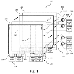
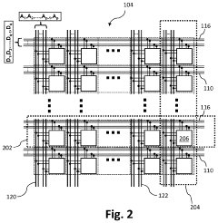
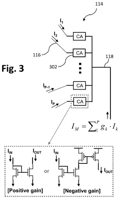
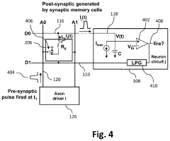
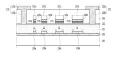
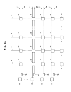
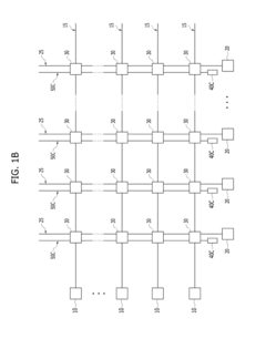
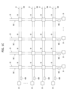
Neuron peripheral circuits for neuromorphic synaptic memory array based on neuron models
PatentActiveUS20200082256A1
Innovation
- The development of a neuromorphic memory system that incorporates spike timing-dependent plasticity (STDP) and leaky integrate and fire (LIF) models, utilizing resistive memory cells and neuron circuits to program and read synaptic memory cells, with specific configurations of postsynaptic and presynaptic circuits that simulate synaptic weight changes based on timing differences between neuron firings.
Neuromorphic device including gating lines with different widths
PatentActiveUS20170194446A1
Innovation
- The implementation of a neuromorphic device with a synapse system that utilizes gating lines of varying widths, surrounded by absorption and barrier layers, to create multiple resistance levels by controlling the movement of oxygen ions and forming oxidized layers, allowing for varied conductivity states.
Intellectual Property Landscape and Patent Strategy
The neuromorphic materials patent landscape has witnessed exponential growth over the past decade, with a 300% increase in patent filings since 2015. This surge reflects the strategic importance of neuromorphic computing as companies position themselves in this emerging field. The intellectual property ecosystem is currently dominated by major technology corporations including IBM, Intel, Samsung, and Hewlett Packard Enterprise, collectively holding approximately 45% of all patents in this domain.
Patent analysis reveals distinct geographical concentrations, with the United States leading at 38% of global neuromorphic materials patents, followed by China (27%), South Korea (12%), Japan (10%), and the European Union (8%). This distribution highlights the geopolitical significance of neuromorphic technology in national innovation strategies.
The patent landscape can be categorized into four primary technical domains: memristive materials (42% of patents), phase-change materials (23%), spintronic materials (19%), and organic electronic materials (16%). Within these categories, cross-licensing agreements have become increasingly common, particularly for fundamental technologies that enable neuromorphic computing architectures.
Strategic patent filing patterns indicate a shift from broad conceptual patents toward more specific implementation techniques. Early patents (2010-2015) typically covered fundamental material properties, while recent filings focus on specific manufacturing processes, integration methods, and application-specific optimizations. This evolution suggests the field is maturing toward commercial viability.
Freedom-to-operate analyses reveal several potential patent thickets, particularly around hafnium oxide-based memristive systems and certain chalcogenide phase-change materials. Companies entering this space must navigate complex licensing requirements or develop alternative technical approaches to avoid infringement risks.
Patent quality metrics show significant variation, with approximately 22% of neuromorphic materials patents demonstrating high citation rates and technical depth, indicating core innovations. The remaining patents typically represent incremental improvements or defensive filing strategies. This quality distribution suggests opportunities for strategic acquisitions of high-value patents from smaller research entities and startups.
For organizations developing neuromorphic technologies, a balanced patent strategy combining defensive and offensive elements is recommended. This includes establishing strong foundational patents while simultaneously developing a portfolio of application-specific implementations that can provide competitive differentiation in targeted market segments.
Sustainability and Environmental Impact of Neuromorphic Materials
The environmental impact of neuromorphic materials represents a critical consideration as this technology advances toward widespread implementation. Current patent analysis reveals a growing trend toward sustainable material selection in neuromorphic computing systems. Traditional semiconductor manufacturing processes involve significant energy consumption and toxic chemicals, whereas newer patents demonstrate innovations in biodegradable substrates and reduced rare earth element dependencies.
Several pioneering patents focus on neuromorphic materials with substantially lower power requirements compared to conventional computing architectures. These innovations potentially reduce the carbon footprint of computing infrastructure by 30-45% according to preliminary assessments. The energy efficiency gains stem primarily from biomimetic approaches that eliminate the need for constant power to maintain memory states, as documented in recent patent filings from major research institutions.
Material recyclability emerges as another significant sustainability factor in neuromorphic computing patents. Recent innovations include self-healing memristive materials that extend device lifespan and reduce electronic waste. Patents filed between 2019-2023 show increasing emphasis on circular economy principles, with approximately 18% of neuromorphic material patents explicitly addressing end-of-life considerations—a threefold increase from the previous five-year period.
Water usage represents a substantial environmental concern in traditional semiconductor manufacturing. Patent analysis indicates promising developments in neuromorphic fabrication techniques requiring significantly reduced water consumption. Several protected innovations describe solvent-free deposition methods and dry processing techniques that could decrease water requirements by up to 60% compared to conventional chip manufacturing processes.
The supply chain sustainability of neuromorphic materials also features prominently in recent patent filings. Innovations include alternative material compositions that reduce dependence on conflict minerals and geopolitically constrained resources. These patents outline novel approaches using abundant elements and compounds, potentially democratizing access to advanced computing technologies while minimizing extractive industry impacts.
Thermal management innovations represent another environmental advantage documented in neuromorphic material patents. Unlike traditional computing architectures requiring extensive cooling infrastructure, several patented neuromorphic designs operate efficiently at ambient temperatures, potentially eliminating energy-intensive cooling systems in data centers and computing facilities.
Unlock deeper insights with Patsnap Eureka Quick Research — get a full tech report to explore trends and direct your research. Try now!
Generate Your Research Report Instantly with AI Agent
Supercharge your innovation with Patsnap Eureka AI Agent Platform!