Perovskite Interface Engineering: Enhancing Stability via Hole/Electron Transport Layers
AUG 20, 20259 MIN READ
Generate Your Research Report Instantly with AI Agent
Patsnap Eureka helps you evaluate technical feasibility & market potential.
Perovskite Interface Goals
Perovskite solar cells have emerged as a promising technology in the field of photovoltaics, offering high efficiency and low-cost manufacturing potential. The primary goal of perovskite interface engineering is to enhance the stability and performance of these devices through the optimization of hole and electron transport layers. This objective addresses one of the most significant challenges facing perovskite solar cells: their long-term stability under various environmental conditions.
A key focus is on developing robust and efficient charge transport layers that can effectively extract and transport charge carriers while simultaneously protecting the perovskite layer from degradation. The hole transport layer (HTL) and electron transport layer (ETL) play crucial roles in this regard, serving as selective contacts for holes and electrons, respectively. Improving the interface between these transport layers and the perovskite absorber is essential for minimizing recombination losses and enhancing overall device efficiency.
Another critical goal is to mitigate the effects of ion migration within the perovskite layer, which can lead to hysteresis and long-term instability. Interface engineering aims to create barrier layers or modify existing transport layers to suppress ion movement and prevent their accumulation at interfaces. This approach not only improves device stability but also enhances reproducibility and reliability in performance metrics.
Researchers are also focusing on developing transport layers that are chemically compatible with the perovskite material, ensuring minimal reactivity and degradation at the interfaces. This includes exploring new materials and compositions for both HTLs and ETLs that can withstand the chemical environment of the perovskite while maintaining their charge transport properties over extended periods.
Furthermore, interface engineering seeks to address the issue of moisture sensitivity in perovskite solar cells. By developing hydrophobic transport layers or incorporating water-repellent additives, researchers aim to create a protective barrier against moisture ingress, significantly improving the device's resistance to environmental degradation.
Lastly, a significant goal of perovskite interface engineering is to develop scalable and industrially viable processes for depositing high-quality transport layers. This includes exploring solution-processable materials and low-temperature deposition techniques that are compatible with flexible substrates and large-area manufacturing processes, paving the way for commercial adoption of perovskite solar cell technology.
Market Demand Analysis
The market demand for perovskite solar cells, particularly those with enhanced stability through interface engineering, has been steadily growing in recent years. This demand is driven by the increasing global focus on renewable energy sources and the need for more efficient and cost-effective solar technologies. Perovskite solar cells have emerged as a promising alternative to traditional silicon-based photovoltaics due to their potential for high efficiency, low production costs, and versatility in applications.
The global solar energy market is projected to expand significantly in the coming years, with perovskite technology poised to capture a substantial share. As governments worldwide implement stricter environmental regulations and set ambitious renewable energy targets, the demand for advanced solar technologies continues to rise. This trend is particularly evident in regions such as Europe, North America, and Asia-Pacific, where investments in clean energy infrastructure are accelerating.
One of the key factors driving market demand for perovskite interface engineering is the need for improved stability and longevity of solar cells. While perovskite solar cells have demonstrated impressive efficiency gains, their long-term stability remains a critical challenge. The development of effective hole and electron transport layers through interface engineering addresses this issue directly, making perovskite technology more attractive for commercial applications.
The building-integrated photovoltaics (BIPV) sector represents a significant market opportunity for perovskite solar cells with enhanced stability. The ability to incorporate these cells into various building materials, such as windows and facades, opens up new avenues for solar energy generation in urban environments. This application requires solar cells that can withstand diverse environmental conditions and maintain performance over extended periods, making stability-enhanced perovskite cells particularly valuable.
Furthermore, the portable electronics and Internet of Things (IoT) markets are showing increasing interest in perovskite solar technology. The lightweight nature and flexibility of perovskite cells, combined with improved stability, make them ideal for powering small devices and sensors in various settings. This expanding application range is expected to drive further demand for advanced perovskite interface engineering solutions.
As the technology matures and demonstrates improved stability and performance, it is anticipated that major solar panel manufacturers will begin incorporating perovskite cells into their product lines. This shift is likely to create a significant market pull for perovskite interface engineering technologies, as manufacturers seek to differentiate their offerings and capture market share in the highly competitive solar energy sector.
Interface Challenges
Perovskite solar cells have shown remarkable potential in the field of photovoltaics, but their widespread adoption is hindered by significant interface challenges. These challenges primarily stem from the complex interactions between the perovskite layer and the charge transport layers, which play a crucial role in device performance and stability.
One of the main interface challenges is the formation of defects at the boundaries between the perovskite and the charge transport layers. These defects can act as recombination centers, reducing the overall efficiency of the solar cell. Additionally, they can serve as pathways for ion migration, leading to degradation of the perovskite material and compromising long-term stability.
Another critical issue is the energy level alignment between the perovskite and the charge transport layers. Improper alignment can result in charge accumulation at the interfaces, leading to increased recombination losses and reduced open-circuit voltage. This misalignment can also contribute to hysteresis effects, which complicate device characterization and reduce overall performance.
The choice of materials for hole and electron transport layers presents its own set of challenges. Many commonly used transport materials are sensitive to moisture and oxygen, which can accelerate degradation of the entire device. Furthermore, some transport layers may react chemically with the perovskite material, forming unwanted compounds at the interface and compromising device stability.
Interface roughness and morphology also play a significant role in device performance. Uneven interfaces can lead to poor contact between layers, resulting in increased series resistance and reduced charge extraction efficiency. Controlling the morphology of the interfaces is particularly challenging due to the solution-processing nature of perovskite solar cells.
The presence of mobile ions in the perovskite layer adds another layer of complexity to interface engineering. These ions can migrate to the interfaces under applied bias or thermal stress, altering the electronic properties of the transport layers and potentially causing reversible or irreversible degradation of the device.
Lastly, the scalability of interface engineering techniques remains a significant challenge. Many successful approaches demonstrated in laboratory settings may not be easily transferable to large-scale manufacturing processes, hindering the commercialization of perovskite solar cells.
Addressing these interface challenges requires a multifaceted approach, combining materials science, device physics, and advanced characterization techniques. Innovative strategies in interface engineering are essential to unlock the full potential of perovskite solar cells and pave the way for their widespread adoption in the renewable energy landscape.
Current Interface Solutions
01 Compositional engineering for stability enhancement
Improving the stability of perovskite solar cells through careful selection and modification of the perovskite material composition. This includes incorporating mixed cations or halides, doping with specific elements, or using additives to enhance the structural and chemical stability of the perovskite layer.- Compositional engineering for stability enhancement: Improving the stability of perovskite solar cells through careful selection and modification of the perovskite material composition. This includes incorporating mixed cations or halides, doping with specific elements, or using additives to enhance the structural and chemical stability of the perovskite layer.
- Encapsulation and barrier layers: Developing effective encapsulation techniques and barrier layers to protect perovskite solar cells from environmental factors such as moisture and oxygen. This involves the use of hydrophobic materials, multi-layer encapsulation strategies, or advanced sealing methods to improve long-term stability.
- Interface engineering: Optimizing the interfaces between different layers in perovskite solar cells to enhance stability. This includes developing novel charge transport materials, passivation layers, or buffer layers that can improve charge extraction while protecting the perovskite layer from degradation.
- Defect passivation and grain boundary engineering: Addressing stability issues related to defects and grain boundaries in perovskite films. This involves developing strategies to passivate defects, control grain size and orientation, or introduce additives that can enhance the structural stability of the perovskite layer.
- Thermal and light stability enhancement: Improving the thermal and light stability of perovskite solar cells to withstand operational conditions. This includes developing heat-resistant materials, incorporating UV filters, or designing device architectures that can better dissipate heat and resist light-induced degradation.
02 Encapsulation and barrier layers
Developing effective encapsulation techniques and barrier layers to protect perovskite solar cells from environmental factors such as moisture and oxygen. This involves the use of hydrophobic materials, multi-layer encapsulation strategies, or advanced sealing methods to improve long-term stability.Expand Specific Solutions03 Interface engineering
Optimizing the interfaces between different layers in perovskite solar cells to enhance stability. This includes developing novel charge transport materials, passivation layers, or buffer layers that can improve charge extraction and reduce interfacial degradation.Expand Specific Solutions04 Defect management and passivation
Implementing strategies to reduce defects and trap states in perovskite materials and at interfaces. This involves developing passivation techniques, using additives to heal defects, or optimizing growth conditions to minimize the formation of detrimental defects that can lead to instability.Expand Specific Solutions05 Thermal and light stability enhancement
Improving the thermal and light stability of perovskite solar cells through material design and device architecture optimization. This includes developing heat-resistant materials, incorporating light-stabilizing additives, or designing structures that can better withstand thermal stress and prolonged light exposure.Expand Specific Solutions
Key Industry Players
The perovskite interface engineering field is in a dynamic growth phase, with significant market potential driven by the global push for renewable energy. The technology is advancing rapidly, but still faces challenges in stability and commercialization. Key players like First Solar, Trina Solar, and LONGi Green Energy are investing heavily in R&D to overcome these hurdles. Academic institutions such as KAUST and EPFL are making breakthrough discoveries, while emerging companies like Oxford Photovoltaics are working to bridge the gap between lab and market. The competitive landscape is diverse, with established solar manufacturers, innovative startups, and research institutions all vying to lead in this promising technology.
Alliance for Sustainable Energy LLC
Technical Solution: The Alliance, which manages the National Renewable Energy Laboratory (NREL), has made substantial contributions to perovskite interface engineering. They have developed a novel interfacial layer using self-assembled monolayers (SAMs) of silane-anchored conjugated organic molecules, which significantly improve the stability and efficiency of perovskite solar cells[7]. NREL researchers have also pioneered the use of quantum dots as interfacial layers, enhancing charge extraction and reducing recombination at the perovskite/transport layer interface[8]. Additionally, they have explored the use of 2D perovskite capping layers to improve moisture resistance and overall device stability[9].
Strengths: Diverse range of interface engineering approaches, strong focus on improving both stability and efficiency. Weaknesses: Some advanced materials may face challenges in large-scale production and cost-effectiveness.
King Abdullah University of Science & Technology
Technical Solution: KAUST has developed a novel approach to perovskite interface engineering by introducing a thin layer of 2D perovskite between the 3D perovskite absorber and the hole transport layer. This 2D/3D heterostructure significantly enhances device stability by suppressing ion migration and reducing defect density at the interface[1]. The team has also explored the use of dopant-free hole transport materials, such as self-assembled monolayers (SAMs), which improve charge extraction and reduce interfacial recombination[2]. Additionally, KAUST researchers have developed a molecular-level passivation strategy using organic halide salts to stabilize the perovskite surface and interfaces, resulting in improved device longevity[3].
Strengths: Innovative approaches to interface engineering, focus on stability enhancement, and use of novel materials. Weaknesses: Potential scalability issues for some techniques and the need for further long-term stability testing in real-world conditions.
Core Interface Innovations
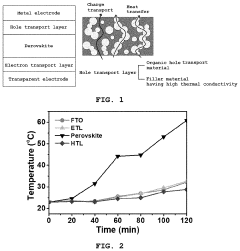
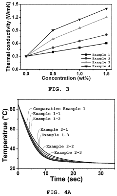
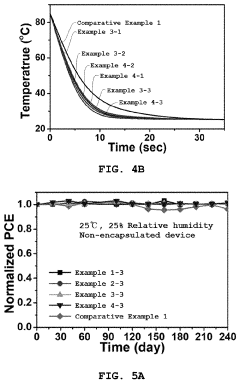
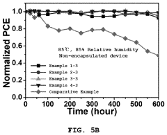
Hole transport layer comprising thermally conductive inorganic structure, perovskite solar cell comprising same, and method of manufacturing same
PatentInactiveUS20210273185A1
Innovation
- A hole transport layer incorporating a thermally conductive inorganic structure with nanoparticles and a hole transport organic material, where the nanoparticles form a porous pathway for heat dissipation and prevent water and oxygen ingress, while maintaining charge transport efficiency.
Perovskite light emitting diode
PatentWO2020111650A1
Innovation
- A conductive conjugated polymer with specific counter ions is used as a hole transport layer, eliminating the need for a separate passivation layer and replacing PEDOT:PSS, thereby reducing defects and improving the stability and performance of the perovskite light-emitting device.


Material Characterization
Material characterization plays a crucial role in understanding and optimizing perovskite interface engineering for enhanced stability through hole and electron transport layers. Various analytical techniques are employed to investigate the physical, chemical, and electronic properties of perovskite materials and their interfaces.
X-ray diffraction (XRD) is widely used to determine the crystal structure and phase purity of perovskite materials. This technique provides valuable information about lattice parameters, crystallite size, and preferred orientation. Additionally, grazing incidence XRD (GIXRD) is particularly useful for studying thin films and interfaces, offering insights into the structural evolution of perovskite layers during device fabrication.
Scanning electron microscopy (SEM) and transmission electron microscopy (TEM) are essential for examining the morphology and microstructure of perovskite films and interfaces. SEM reveals surface topography and grain size distribution, while TEM provides high-resolution imaging of interface regions and atomic-scale defects. Energy-dispersive X-ray spectroscopy (EDS) coupled with these microscopy techniques enables elemental mapping and composition analysis.
Atomic force microscopy (AFM) is employed to investigate surface roughness and topography of perovskite films and transport layers. This technique can also be used to measure local electrical properties through conductive AFM (c-AFM) and Kelvin probe force microscopy (KPFM), providing insights into charge transport mechanisms and interfacial energy alignment.
Spectroscopic techniques such as UV-visible spectroscopy and photoluminescence (PL) are utilized to study the optical properties of perovskite materials. These methods offer information about bandgap, absorption coefficients, and charge carrier dynamics. Time-resolved PL measurements are particularly valuable for investigating charge transfer processes at perovskite interfaces.
X-ray photoelectron spectroscopy (XPS) and ultraviolet photoelectron spectroscopy (UPS) are powerful tools for analyzing the chemical composition and electronic structure of perovskite surfaces and interfaces. These techniques provide information about elemental composition, oxidation states, and energy level alignment between perovskite and transport layers.
Impedance spectroscopy is employed to study charge transport and recombination processes in perovskite solar cells. This technique allows for the investigation of interfacial charge transfer resistance and capacitance, providing insights into the effectiveness of hole and electron transport layers in enhancing device stability.
Advanced characterization methods such as synchrotron-based X-ray techniques (e.g., GIWAXS, EXAFS) and neutron scattering offer unique capabilities for probing perovskite interfaces at various length scales. These techniques provide valuable information about crystal structure, defects, and ion migration processes that influence device stability.
Scalability Assessment
Scalability assessment is a critical aspect of perovskite interface engineering, particularly in the context of enhancing stability through hole and electron transport layers. The transition from laboratory-scale devices to large-area modules and commercial production presents significant challenges that must be addressed to realize the full potential of perovskite solar cells.
One of the primary considerations in scalability is the uniformity of thin film deposition across larger areas. While spin-coating and other solution-based methods are effective for small-scale devices, they become increasingly problematic as the substrate size increases. Alternative deposition techniques such as slot-die coating, blade coating, and spray coating are being explored to achieve consistent film quality over larger areas. These methods must be optimized to ensure uniform thickness and composition of both the perovskite layer and the charge transport layers.
The choice of materials for hole and electron transport layers also plays a crucial role in scalability. Some materials that perform well in small devices may not be suitable for large-scale production due to cost, availability, or processing requirements. Researchers are focusing on developing transport layer materials that are not only effective in enhancing stability but also compatible with large-scale manufacturing processes. Inorganic transport layers, such as nickel oxide for hole transport and tin oxide for electron transport, are gaining attention due to their potential for improved scalability and stability.
Another key aspect of scalability is the development of interconnection strategies for large-area modules. As individual cell size increases, series resistance losses become more significant, necessitating effective module designs that balance performance and manufacturability. Laser scribing and mechanical scribing techniques are being refined to create efficient monolithic interconnections in large-area perovskite modules.
Environmental control during manufacturing is another critical factor in scaling up perovskite solar cell production. The sensitivity of perovskite materials to moisture and oxygen requires careful management of the production environment. Developing cost-effective encapsulation methods that can be applied at scale is essential for long-term stability and commercial viability.
Lastly, the scalability assessment must consider the environmental impact and sustainability of large-scale production. This includes evaluating the availability and toxicity of raw materials, energy consumption during manufacturing, and end-of-life recycling strategies. As the industry moves towards commercialization, these factors will become increasingly important in determining the overall feasibility and market acceptance of perovskite solar technology.
Unlock deeper insights with Patsnap Eureka Quick Research — get a full tech report to explore trends and direct your research. Try now!
Generate Your Research Report Instantly with AI Agent
Supercharge your innovation with Patsnap Eureka AI Agent Platform!