Scalability of photodiode technology in mass production
AUG 21, 20259 MIN READ
Generate Your Research Report Instantly with AI Agent
Patsnap Eureka helps you evaluate technical feasibility & market potential.
Photodiode Tech Evolution
Photodiode technology has undergone significant evolution since its inception in the early 20th century. The journey began with the discovery of the photoelectric effect by Heinrich Hertz in 1887, which laid the foundation for photodiode development. In the 1940s, the first practical silicon photodiodes were created, marking a crucial milestone in the field.
The 1960s saw rapid advancements with the introduction of PIN photodiodes, offering improved sensitivity and faster response times. This period also witnessed the development of avalanche photodiodes (APDs), which provided internal gain mechanisms, enhancing their ability to detect weak light signals.
The 1970s and 1980s brought about further refinements in photodiode technology, including the creation of Schottky photodiodes and the improvement of quantum efficiency. These advancements expanded the spectral range and sensitivity of photodiodes, making them suitable for a wider array of applications.
The 1990s marked the beginning of the integration era, with photodiodes being incorporated into larger optoelectronic systems. This integration paved the way for applications in fiber-optic communications, medical imaging, and consumer electronics.
The turn of the millennium saw a focus on miniaturization and cost reduction, driven by the growing demand for photodiodes in mobile devices and automotive sensors. This period also witnessed the development of back-illuminated photodiodes, which offered superior quantum efficiency and reduced noise levels.
In recent years, the evolution of photodiode technology has been characterized by a push towards higher performance and scalability in mass production. Key areas of focus include improving quantum efficiency, reducing dark current, and enhancing response speed. The development of new materials and fabrication techniques has played a crucial role in addressing these challenges.
Current trends in photodiode technology evolution include the exploration of novel materials such as graphene and other 2D materials for enhanced sensitivity and broader spectral response. Additionally, there is a growing interest in developing photodiodes for specific wavelength ranges, particularly in the infrared and ultraviolet regions, to cater to emerging applications in environmental monitoring and security.
The scalability of photodiode technology in mass production has become a critical focus area, driven by the increasing demand for these devices in various industries. Efforts are being made to optimize manufacturing processes, improve yield rates, and develop more cost-effective production techniques to meet the growing market needs while maintaining high-quality standards.
Market Demand Analysis
The market demand for photodiode technology in mass production has been experiencing significant growth, driven by the increasing adoption of photodiodes in various applications across multiple industries. The automotive sector has emerged as a key driver of demand, with the integration of advanced driver assistance systems (ADAS) and autonomous driving technologies requiring high-performance photodiodes for LiDAR and other sensing applications. This trend is expected to continue as vehicle electrification and automation progress.
Consumer electronics represent another major market segment for photodiodes, with smartphones, tablets, and wearable devices incorporating these components for proximity sensing, ambient light detection, and facial recognition features. The growing popularity of augmented reality (AR) and virtual reality (VR) technologies is further fueling demand for miniaturized, high-sensitivity photodiodes.
In the industrial sector, photodiodes play a crucial role in automation and quality control processes. Machine vision systems, used for inspection and sorting in manufacturing, rely heavily on photodiode technology. The ongoing trend towards Industry 4.0 and smart factories is expected to drive further adoption of photodiodes in industrial applications.
The healthcare and medical devices industry also contributes significantly to the market demand for photodiodes. Applications such as pulse oximetry, blood glucose monitoring, and medical imaging systems require high-performance photodiodes. As telemedicine and remote patient monitoring gain traction, the demand for portable medical devices incorporating photodiode technology is likely to increase.
The telecommunications sector continues to be a steady source of demand for photodiodes, particularly in fiber-optic communication systems. The ongoing rollout of 5G networks and the increasing need for high-speed data transmission are driving the demand for advanced photodiodes in this sector.
Environmental monitoring and scientific research applications also contribute to the market demand, with photodiodes being used in spectroscopy, radiation detection, and atmospheric sensing instruments. The growing focus on climate change and environmental protection is expected to further boost demand in this segment.
As the Internet of Things (IoT) ecosystem expands, the integration of photodiodes in smart home devices, building automation systems, and urban infrastructure is creating new market opportunities. This trend is likely to accelerate as cities worldwide invest in smart city initiatives.
The global photodiode market is projected to grow at a compound annual growth rate (CAGR) of over 8% in the coming years, with Asia-Pacific region leading in terms of both production and consumption. The increasing focus on miniaturization, improved sensitivity, and cost-effective manufacturing processes is driving innovation in photodiode technology to meet the diverse and growing market demands across various industries.
Scalability Challenges
The scalability of photodiode technology in mass production faces several significant challenges that need to be addressed to ensure efficient and cost-effective manufacturing processes. One of the primary obstacles is maintaining consistent quality and performance across large-scale production runs. As the production volume increases, it becomes increasingly difficult to maintain uniform characteristics such as spectral response, dark current, and quantum efficiency across all manufactured devices.
Material consistency is another critical factor affecting scalability. The semiconductor materials used in photodiode fabrication, such as silicon, germanium, or compound semiconductors, must be of high purity and uniformity. Ensuring a stable supply of these materials with consistent properties becomes more challenging as production scales up, potentially leading to variations in device performance and yield rates.
Process control and optimization present ongoing challenges in mass production scenarios. The fabrication of photodiodes involves multiple complex steps, including wafer preparation, doping, metallization, and packaging. Each of these processes must be precisely controlled and optimized for large-scale production, requiring sophisticated equipment and highly skilled personnel. Maintaining tight process control becomes increasingly difficult as production volumes grow, potentially leading to increased defect rates and reduced overall yield.
Miniaturization and integration demands pose additional scalability challenges. As electronic devices continue to shrink in size, there is a growing need for smaller, more integrated photodiodes. Scaling down the size of photodiodes while maintaining or improving their performance characteristics requires advanced manufacturing techniques and materials. This scaling process often introduces new technical hurdles that must be overcome to achieve mass production viability.
Testing and quality assurance processes also become more complex and time-consuming as production scales up. Developing efficient, automated testing procedures that can accurately assess the performance of large numbers of photodiodes is crucial for maintaining product quality and reliability. However, implementing such systems can be technically challenging and resource-intensive.
Cost management is a persistent challenge in scaling photodiode production. While increased production volumes can lead to economies of scale, the initial capital investment required for scaling up manufacturing facilities and equipment can be substantial. Balancing these upfront costs with long-term production efficiencies is critical for maintaining competitiveness in the market.
Environmental considerations and regulatory compliance add another layer of complexity to scalability efforts. As production volumes increase, so does the potential environmental impact of manufacturing processes. Adhering to evolving environmental regulations and implementing sustainable production practices while maintaining cost-effectiveness and efficiency is an ongoing challenge for manufacturers.
Addressing these scalability challenges requires a multifaceted approach, combining advancements in materials science, process engineering, automation technologies, and quality control methodologies. Continuous innovation and investment in research and development are essential to overcome these obstacles and enable the successful mass production of high-quality photodiodes.
Current Manufacturing
01 Scalable photodiode array structures
Advancements in photodiode array structures allow for improved scalability in imaging applications. These structures can be designed to optimize light collection efficiency and reduce crosstalk between adjacent pixels. Scalable designs enable the production of larger sensor arrays while maintaining high performance and sensitivity.- Scalable photodiode array structures: Advancements in photodiode array structures allow for improved scalability in imaging applications. These designs incorporate novel architectures that enable efficient scaling of photodiode arrays, resulting in enhanced performance and resolution for large-scale imaging systems. The scalable structures can be implemented in various configurations to suit different application requirements.
- Integration of photodiodes with CMOS technology: The integration of photodiodes with CMOS technology enables the development of highly scalable and compact image sensors. This approach combines the light-sensing capabilities of photodiodes with the processing power of CMOS circuits, allowing for efficient signal processing and readout. The integration facilitates the creation of high-density pixel arrays suitable for various imaging applications.
- Scalable manufacturing processes for photodiodes: Advancements in manufacturing processes have improved the scalability of photodiode production. These processes include optimized deposition techniques, precise doping methods, and innovative packaging solutions. The scalable manufacturing approaches enable cost-effective production of large quantities of photodiodes while maintaining consistent performance and quality.
- Scalable readout circuits for large photodiode arrays: Development of scalable readout circuits is crucial for handling large photodiode arrays efficiently. These circuits are designed to process and transmit signals from numerous photodiodes simultaneously, enabling the creation of high-resolution imaging systems. The scalable readout architectures optimize power consumption and data throughput for improved overall system performance.
- Software-based scalability solutions for photodiode systems: Software-based approaches enhance the scalability of photodiode systems by providing flexible data processing and analysis capabilities. These solutions include advanced algorithms for signal processing, image reconstruction, and system calibration. The software-based scalability allows for easy adaptation to different photodiode array sizes and configurations, improving system versatility and performance.
02 Integration of photodiodes with CMOS technology
The integration of photodiodes with CMOS technology enables the creation of highly scalable image sensors. This approach allows for the fabrication of compact, low-power devices that can be easily scaled up for larger applications. The combination of photodiodes and CMOS circuitry on a single chip improves overall system performance and reduces manufacturing costs.Expand Specific Solutions03 Advanced manufacturing techniques for photodiode scalability
Novel manufacturing techniques have been developed to enhance the scalability of photodiode production. These methods include improved wafer-level processing, advanced packaging technologies, and innovative materials integration. Such techniques enable the mass production of high-quality photodiodes with consistent performance across large-scale arrays.Expand Specific Solutions04 Scalable readout circuits for large photodiode arrays
Scalable readout circuits are crucial for managing large photodiode arrays efficiently. These circuits are designed to handle increased data throughput from expanded sensor arrays while maintaining high speed and low noise performance. Advanced readout architectures enable the scaling of photodiode arrays to meet the demands of high-resolution imaging applications.Expand Specific Solutions05 Photodiode scaling for improved sensitivity and dynamic range
Scaling techniques for photodiodes focus on enhancing sensitivity and expanding dynamic range. These approaches involve optimizing the photodiode structure, improving light collection efficiency, and implementing advanced noise reduction methods. By addressing these factors, photodiode technology can be scaled to meet the requirements of increasingly demanding imaging applications.Expand Specific Solutions
Key Industry Players
The scalability of photodiode technology in mass production is at a mature stage, with significant market growth potential. The global photodiode market is expected to expand due to increasing demand in various applications, including telecommunications, automotive, and consumer electronics. Technologically, companies like Corning, FUJIFILM, and NEC are leading innovation in photodiode manufacturing processes, improving efficiency and reducing costs. Emerging players such as Seoul Viosys and Xiamen Changelight are also contributing to advancements in the field. The industry is characterized by ongoing research and development efforts, with academic institutions like MIT and Fudan University collaborating with industry partners to push the boundaries of photodiode technology and enhance scalability for mass production.
Corning, Inc.
Technical Solution: Corning has developed advanced photodiode technology for mass production, focusing on improving scalability and performance. Their approach involves using proprietary glass substrates and precision manufacturing techniques to create high-quality photodiodes with consistent characteristics. Corning's process allows for the production of large-area photodiodes with uniform response and low dark current. They have implemented automated inspection and testing systems to ensure quality control during mass production, significantly reducing defects and improving yield rates[1][3]. Additionally, Corning has developed novel packaging solutions that enhance the durability and reliability of photodiodes in various environmental conditions, making them suitable for a wide range of applications from consumer electronics to industrial sensors[2].
Strengths: High-quality, consistent photodiodes; scalable production process; advanced packaging solutions. Weaknesses: Potentially higher production costs; may require specialized equipment for manufacturing.
Massachusetts Institute of Technology
Technical Solution: MIT researchers have developed innovative approaches to enhance the scalability of photodiode technology for mass production. Their work focuses on novel materials and fabrication techniques to improve photodiode performance and manufacturability. One significant advancement is the development of flexible, large-area photodiodes using organic semiconductors and roll-to-roll fabrication processes[13]. This approach allows for high-throughput production of photodiodes on flexible substrates, opening up new applications in wearable electronics and large-area sensors. MIT has also explored the use of quantum dot materials to create spectrally tunable photodiodes that can be easily integrated into existing silicon-based manufacturing processes[14]. Additionally, they have developed advanced computational models to optimize photodiode designs for specific applications, streamlining the development process and improving yield in mass production[15].
Strengths: Innovative materials and fabrication techniques; potential for flexible and large-area photodiodes; advanced design optimization. Weaknesses: Some technologies may still be in early stages of development; potential challenges in scaling up novel material production.
Innovative Scaling
Rear surface irradiation photodiode array and method for producing the same
PatentWO2003096427A1
Innovation
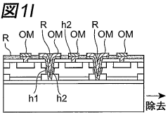
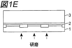
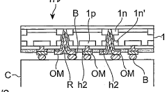
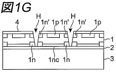
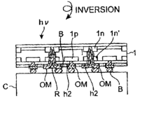
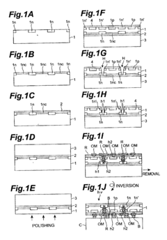
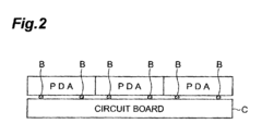
- A method involving forming high-concentration impurity regions on both sides of a semiconductor substrate, thinning one surface, and connecting them through holes, with resin embedding to enhance strength, allowing for efficient electrical connection and mass production of back-illuminated photodiode arrays.
Back illuminated photodiode array and method of manufacturing the same
PatentInactiveUS6933489B2
Innovation
- A method involving forming high concentration impurity regions on both sides of a semiconductor substrate, thinning one side, creating holes to connect these regions, and burying resin in the holes to enhance strength, allowing for industrial mass production of back illuminated photodiode arrays with improved signal-to-noise ratio and precision.
Supply Chain Analysis
The supply chain for photodiode mass production is a complex network involving multiple stakeholders and processes. Raw material suppliers play a crucial role, providing high-purity semiconductors such as silicon, germanium, or compound materials like gallium arsenide. These materials form the foundation of photodiode manufacturing and their quality directly impacts device performance.
Component manufacturers are responsible for producing various parts of the photodiode, including the semiconductor wafers, metal contacts, and protective packaging. The precision and consistency of these components are essential for maintaining product quality across large production volumes.
Specialized equipment suppliers provide the necessary tools for photodiode fabrication, including photolithography systems, ion implanters, and chemical vapor deposition machines. The availability and reliability of this equipment significantly influence production capacity and yield rates.
Assembly and testing facilities are integral to the supply chain, ensuring that individual components are correctly integrated and that finished photodiodes meet specified performance criteria. These facilities often employ automated systems to handle the high volumes required for mass production.
Logistics and distribution networks facilitate the movement of raw materials, components, and finished products throughout the supply chain. Efficient inventory management and just-in-time delivery systems are crucial for maintaining production flow and minimizing costs.
Quality control measures are implemented at various stages of the supply chain to maintain consistency and reliability in mass-produced photodiodes. This includes incoming material inspection, in-process testing, and final product verification.
The scalability of photodiode technology in mass production heavily depends on the robustness and flexibility of the supply chain. Challenges include managing lead times for specialized materials, adapting to fluctuations in demand, and ensuring consistent quality across large production runs.
To enhance scalability, manufacturers often employ strategies such as vertical integration, strategic partnerships with key suppliers, and the development of alternative sourcing options. Advanced supply chain management systems and predictive analytics are increasingly used to optimize inventory levels and production schedules.
As the demand for photodiodes continues to grow in various applications, including consumer electronics, automotive sensors, and medical devices, the supply chain must evolve to support higher volumes and potentially new materials or manufacturing processes. This may involve investments in new production facilities, the development of more efficient fabrication techniques, and the exploration of novel materials that can be more easily scaled for mass production.
Quality Control
Quality control is a critical aspect of scaling photodiode technology in mass production. As production volumes increase, maintaining consistent quality becomes increasingly challenging. Effective quality control measures are essential to ensure that each photodiode meets the required specifications and performance standards.
One key element of quality control in photodiode mass production is the implementation of automated inspection systems. These systems utilize advanced imaging and spectroscopic techniques to detect defects and variations in the photodiode structure, such as surface irregularities, contamination, or inconsistencies in the semiconductor layers. By integrating these inspection systems throughout the production line, manufacturers can identify and address issues in real-time, minimizing the risk of defective products reaching the market.
Statistical process control (SPC) plays a crucial role in maintaining quality during large-scale production. By continuously monitoring key parameters and performance metrics, manufacturers can detect trends and variations that may indicate potential quality issues. This data-driven approach allows for proactive adjustments to the production process, ensuring consistent output quality across large batches.
Standardization of production processes and materials is another vital component of quality control in photodiode mass production. Establishing and adhering to strict protocols for material sourcing, handling, and processing helps minimize variations between production runs. This includes maintaining precise control over factors such as temperature, humidity, and cleanliness in the production environment.
Testing and characterization of photodiodes at various stages of production are essential for ensuring quality. This includes both in-line testing during the manufacturing process and final product testing. Key parameters such as responsivity, dark current, and spectral response must be measured and verified to meet specified tolerances. As production scales up, the development of high-throughput testing methods becomes increasingly important to maintain efficiency without compromising quality.
Traceability and documentation are critical aspects of quality control in mass production. Implementing robust systems for tracking materials, processes, and test results throughout the production cycle enables manufacturers to quickly identify and isolate potential quality issues. This level of traceability is particularly important in industries with stringent regulatory requirements, such as medical devices or aerospace applications.
Continuous improvement initiatives are essential for maintaining and enhancing quality control as production scales. This involves regularly reviewing and updating quality control processes, investing in new technologies for inspection and testing, and providing ongoing training for personnel involved in production and quality assurance.
Unlock deeper insights with Patsnap Eureka Quick Research — get a full tech report to explore trends and direct your research. Try now!
Generate Your Research Report Instantly with AI Agent
Supercharge your innovation with Patsnap Eureka AI Agent Platform!
