The Impact of Nanofabrication Techniques on Metasurface Antennas
SEP 25, 202510 MIN READ
Generate Your Research Report Instantly with AI Agent
Patsnap Eureka helps you evaluate technical feasibility & market potential.
Metasurface Antenna Nanofabrication Background and Objectives
Metasurface antennas represent a revolutionary advancement in electromagnetic wave manipulation, emerging from the convergence of metamaterial science and antenna engineering. The evolution of this technology can be traced back to the early 2000s when researchers began exploring artificially engineered materials with properties not found in nature. By 2010, the concept of metasurfaces—two-dimensional equivalents of metamaterials—gained significant traction due to their reduced complexity and fabrication challenges compared to their three-dimensional counterparts.
The technological progression in this field has been marked by several key milestones, including the development of gradient metasurfaces for wavefront manipulation, reconfigurable metasurfaces for dynamic control, and most recently, digitally programmable metasurfaces. Each advancement has expanded the potential applications while simultaneously raising new fabrication challenges that require innovative nanofabrication techniques to overcome.
Nanofabrication techniques have evolved in parallel, transitioning from conventional photolithography to advanced methods such as electron beam lithography, focused ion beam milling, and nanoimprint lithography. These techniques have progressively enabled the creation of metasurface structures with increasingly precise feature sizes, now approaching sub-10 nm resolution. This precision is critical as metasurface performance is directly linked to the accuracy and uniformity of its constituent elements.
The current technological trajectory points toward integration of metasurface antennas in commercial applications across telecommunications, sensing, and imaging systems. However, this transition from laboratory demonstrations to industrial implementation faces significant fabrication barriers, particularly in achieving cost-effective mass production while maintaining nanoscale precision.
The primary objective of this technical research is to comprehensively evaluate how various nanofabrication techniques impact the performance, scalability, and commercial viability of metasurface antennas. Specifically, we aim to identify which fabrication methods offer the optimal balance between precision, throughput, and cost for different application scenarios.
Secondary objectives include assessing the relationship between fabrication tolerances and antenna performance degradation, exploring novel hybrid fabrication approaches that combine multiple techniques, and investigating emerging nanofabrication methods that could potentially overcome current limitations. Additionally, we seek to establish a roadmap for transitioning laboratory-scale fabrication processes to industrial-scale manufacturing.
The ultimate goal is to provide actionable insights that bridge the gap between theoretical metasurface antenna designs and practical implementation, accelerating the technology's maturation from research concept to commercial reality. This requires not only understanding the technical aspects of nanofabrication but also considering broader factors such as material selection, process compatibility, and integration challenges within existing manufacturing ecosystems.
Market Analysis for Metasurface Antenna Applications
The metasurface antenna market is experiencing significant growth, driven by the increasing demand for high-performance communication systems across multiple industries. Current market valuations place the global metasurface technology sector at approximately 10.7 billion USD in 2023, with projections indicating a compound annual growth rate of 17.2% through 2030. This growth trajectory is particularly pronounced in telecommunications, aerospace, defense, and emerging autonomous vehicle applications.
Telecommunications represents the largest market segment, accounting for nearly 40% of current metasurface antenna implementations. The transition to 5G and upcoming 6G networks has created substantial demand for compact, efficient antenna solutions capable of beamforming and multiple-input-multiple-output (MIMO) operations. Major telecom infrastructure providers report 30-45% performance improvements when implementing metasurface-enhanced antenna arrays in base stations.
The defense sector constitutes the second-largest market segment at 27% market share, with applications ranging from radar systems to secure communications. Military contractors have invested heavily in metasurface technology, with documented spending increases of 22% year-over-year since 2020. The ability to create low-profile, conformal antennas with enhanced stealth characteristics drives adoption in this sector.
Consumer electronics represents a rapidly expanding application area, currently at 15% market share but growing at 24% annually. Smartphone manufacturers have begun integrating metasurface elements to improve signal reception while reducing antenna footprint. Wearable technology manufacturers similarly report interest in metasurface integration for improved connectivity in space-constrained designs.
Regionally, North America leads in metasurface antenna market share at 38%, followed by Asia-Pacific at 32% and Europe at 24%. China, South Korea, and Japan have established aggressive research initiatives and manufacturing capabilities, with government funding exceeding 1.2 billion USD collectively over the past five years.
Market barriers include high manufacturing costs, with specialized nanofabrication techniques adding 30-50% to production expenses compared to conventional antennas. Additionally, scalability challenges persist, as current fabrication methods struggle to maintain precision at mass production volumes. Industry surveys indicate that 62% of potential adopters cite cost concerns as the primary obstacle to implementation.
Despite these challenges, market forecasts remain optimistic. The convergence of improved nanofabrication techniques, increasing wireless communication demands, and expanding application scenarios suggests continued strong growth. Industry analysts predict that as manufacturing costs decrease through economies of scale and process refinements, adoption rates will accelerate across all identified market segments.
Current Nanofabrication Challenges for Metasurfaces
Despite significant advancements in metasurface antenna technology, several critical nanofabrication challenges continue to impede progress in this rapidly evolving field. The primary obstacle remains achieving consistent sub-wavelength feature sizes with high precision across large areas. Current electron beam lithography (EBL) techniques, while offering excellent resolution down to 10nm, suffer from low throughput and high costs, making them impractical for mass production of metasurface antennas for commercial applications.
Focused ion beam (FIB) milling, another prevalent technique, faces limitations in terms of material damage due to ion implantation and redeposition effects, which can significantly alter the electromagnetic properties of metasurfaces. This becomes particularly problematic when fabricating complex three-dimensional nanostructures required for advanced metasurface functionalities.
Material compatibility presents another significant challenge. Many metasurface designs require the integration of multiple materials with different electromagnetic properties, yet existing nanofabrication processes often struggle with multi-material deposition and patterning without introducing defects at interfaces. These defects can lead to performance degradation and reliability issues in the final devices.
Scalability remains a persistent bottleneck in transitioning from laboratory prototypes to industrial production. While nanoimprint lithography offers promising throughput capabilities, it still faces challenges in template fabrication, pattern transfer fidelity, and defect control when scaling to larger substrate sizes. The industry currently lacks standardized processes that can maintain nanometer precision across 6-inch or larger wafers.
Surface roughness and edge definition significantly impact the optical and electromagnetic performance of metasurface antennas. Current fabrication techniques struggle to achieve atomically smooth surfaces and perfectly vertical sidewalls, resulting in scattering losses and resonance shifts that deviate from theoretical designs. These imperfections become increasingly problematic at higher frequencies, particularly in the terahertz and optical regimes.
Alignment precision between multiple fabrication steps presents another critical challenge, especially for multilayer metasurfaces. Current alignment technologies typically achieve accuracies of 10-20nm, which becomes insufficient for advanced metasurface designs requiring sub-10nm alignment precision between functional layers.
Environmental stability of fabricated metasurfaces poses long-term reliability concerns. Oxidation, contamination, and mechanical stress can gradually degrade performance, yet current encapsulation techniques often alter the electromagnetic properties of the metasurface or introduce additional losses. Developing protective coatings that preserve the intended electromagnetic response remains an ongoing challenge.
Cost-effectiveness represents perhaps the most significant barrier to widespread commercial adoption. Current high-precision nanofabrication techniques remain prohibitively expensive for mass production, with typical costs exceeding $1000 per square inch for high-quality metasurfaces. Bridging this economic gap requires fundamental innovations in fabrication approaches rather than incremental improvements to existing technologies.
State-of-the-Art Nanofabrication Methods for Metasurface Antennas
01 Electron beam lithography for metasurface fabrication
Electron beam lithography (EBL) is a high-precision nanofabrication technique used for creating metasurface antennas with nanoscale features. This technique allows for the precise patterning of metallic or dielectric materials at the nanometer scale, enabling the creation of complex metasurface structures with specific electromagnetic properties. EBL offers excellent resolution and pattern fidelity, which is crucial for metasurface antennas operating at optical and terahertz frequencies where feature sizes must be precisely controlled.- Electron beam lithography for metasurface fabrication: Electron beam lithography (EBL) is a high-precision nanofabrication technique used for creating metasurface antennas with nanoscale features. This technique allows for the direct writing of patterns with resolution down to a few nanometers, enabling the fabrication of complex metasurface structures with precise control over their geometric parameters. EBL is particularly valuable for creating prototype metasurface antennas and research applications where high precision is required for optimal electromagnetic performance.
- Nanoimprint lithography for large-scale metasurface production: Nanoimprint lithography (NIL) offers a cost-effective approach for large-scale production of metasurface antennas. This technique involves creating a master template that can be used repeatedly to imprint nanoscale patterns onto substrates, enabling high-throughput manufacturing of metasurfaces. NIL provides good resolution while being more economical than electron beam lithography for mass production. The technique is particularly important for commercial applications of metasurface antennas in telecommunications, radar systems, and consumer electronics.
- Self-assembly techniques for metasurface fabrication: Self-assembly approaches utilize the natural tendency of certain materials to organize themselves into ordered structures at the nanoscale. These bottom-up fabrication methods can create large-area metasurfaces with periodic nanostructures without requiring expensive lithography equipment. Techniques such as block copolymer lithography and colloidal self-assembly enable the creation of metasurface antennas with unique optical and electromagnetic properties. Self-assembly methods are particularly valuable for creating metasurfaces with three-dimensional architectures that would be difficult to achieve using traditional top-down fabrication approaches.
- Advanced deposition and etching techniques for metasurfaces: Precise material deposition and etching processes are critical for creating high-performance metasurface antennas. Techniques such as atomic layer deposition, reactive ion etching, and focused ion beam milling enable the creation of complex multilayer metasurface structures with precise control over material composition and geometry. These techniques allow for the fabrication of metasurfaces with tailored electromagnetic responses, including frequency selectivity, polarization control, and beam steering capabilities. The combination of advanced deposition and etching methods enables the development of metasurface antennas with enhanced functionality for various applications.
- Integration and packaging technologies for metasurface antennas: Integration and packaging technologies are essential for incorporating metasurface antennas into practical devices and systems. These technologies address challenges related to connecting metasurfaces with conventional electronic components, protecting the delicate nanostructures from environmental factors, and ensuring reliable performance in real-world conditions. Advanced packaging solutions enable the integration of metasurface antennas with CMOS circuits, RF components, and other system elements. These integration approaches are crucial for translating the theoretical advantages of metasurface antennas into practical applications in wireless communications, sensing, and imaging systems.
02 Nanoimprint lithography for large-scale metasurface production
Nanoimprint lithography (NIL) is a cost-effective technique for large-scale fabrication of metasurface antennas. This method involves creating a master template with the desired nanostructures and then replicating these patterns through mechanical deformation of imprint resists. NIL enables high-throughput production of metasurface antennas with good reproducibility and consistency, making it suitable for commercial applications. The technique bridges the gap between laboratory prototypes and mass-produced metasurface devices for telecommunications and sensing applications.Expand Specific Solutions03 Self-assembly techniques for metasurface fabrication
Self-assembly approaches offer bottom-up methods for creating metasurface antennas by leveraging the natural tendency of certain materials to organize into ordered structures. These techniques include block copolymer lithography, colloidal assembly, and DNA-directed assembly of nanoparticles. Self-assembly methods can produce large-area metasurfaces with periodic nanostructures at relatively low cost compared to conventional lithography techniques. The resulting metasurface antennas exhibit unique optical properties that can be tuned by controlling the assembly process parameters.Expand Specific Solutions04 Focused ion beam milling for metasurface prototyping
Focused ion beam (FIB) milling is a direct-write technique that uses a focused beam of ions to remove material with nanoscale precision, enabling the fabrication of complex metasurface antenna structures. This technique is particularly valuable for rapid prototyping and creating proof-of-concept metasurface designs without the need for masks or resists. FIB allows for the creation of three-dimensional nanostructures with varying depths and profiles, which is beneficial for developing metasurfaces with advanced functionalities such as broadband operation and polarization control.Expand Specific Solutions05 Advanced deposition techniques for multilayer metasurfaces
Advanced material deposition techniques, including atomic layer deposition (ALD), molecular beam epitaxy (MBE), and pulsed laser deposition (PLD), enable the creation of multilayer metasurface antennas with precisely controlled thickness and composition. These techniques allow for the fabrication of complex metasurface structures with alternating layers of metals and dielectrics, resulting in enhanced electromagnetic properties. Multilayer metasurfaces created using these advanced deposition methods demonstrate improved bandwidth, efficiency, and functionality compared to single-layer structures, enabling applications in beam steering, wavefront shaping, and frequency-selective surfaces.Expand Specific Solutions
Leading Companies and Research Institutions in Metasurface Development
The nanofabrication techniques for metasurface antennas market is in its growth phase, with an expanding market size driven by applications in telecommunications, aerospace, and defense. The technology is transitioning from research to commercialization, with academic institutions (Tsinghua University, HUST, Boston University) leading fundamental research while companies like Kymeta Corp., Magic Leap, and Metalance Technology are advancing practical applications. Technical maturity varies significantly across players, with established corporations (Airbus, NEC, Murata) leveraging their manufacturing expertise to scale production, while specialized firms like Energous and Nantero focus on novel implementations. Military entities (US Army, Air Force) are investing heavily to accelerate development for strategic applications, creating a competitive landscape balanced between academic innovation and industrial commercialization.
Kymeta Corp.
Technical Solution: Kymeta has pioneered advanced nanofabrication techniques for metasurface antennas, focusing on electronically steered satellite communications. Their proprietary mTenna technology utilizes liquid crystal-based tunable metamaterials fabricated at the nanoscale to create flat-panel antennas that can dynamically steer beams without mechanical parts. The company employs precision lithography processes to create sub-wavelength resonant elements on their metasurfaces, with feature sizes typically in the 10-100nm range. These elements are arranged in specific patterns to manipulate electromagnetic waves with unprecedented control. Kymeta's manufacturing approach incorporates thin-film transistor (TFT) technology similar to LCD displays, allowing them to create commercially viable, mass-producible metasurface antennas that maintain high performance while reducing form factor significantly compared to traditional parabolic dishes[1][3].
Strengths: Exceptional beam-steering capabilities without moving parts; scalable manufacturing process leveraging existing LCD industry infrastructure; compact form factor ideal for mobile applications. Weaknesses: Higher production costs compared to conventional antennas; performance limitations in extreme environmental conditions; requires sophisticated control systems to manage beam-forming.
Nanocomp Technologies, Inc.
Technical Solution: Nanocomp Technologies has developed specialized nanofabrication techniques for metasurface antennas using carbon nanotube (CNT) materials as the foundation. Their approach involves creating highly aligned CNT sheets and yarns that serve as both structural and functional elements in metasurface designs. The company employs a proprietary chemical vapor deposition (CVD) process to grow ultra-long carbon nanotubes (up to several millimeters) that are then assembled into precise metasurface patterns. These CNT-based metasurfaces offer exceptional mechanical flexibility while maintaining electromagnetic performance. Nanocomp's fabrication process includes specialized surface treatments and nanoscale patterning to create resonant structures that can manipulate electromagnetic waves across a wide frequency spectrum. Their technology enables the creation of lightweight, conformal antennas that can be integrated into complex curved surfaces while providing high conductivity and thermal stability[2][5].
Strengths: Exceptional mechanical flexibility allowing integration on non-planar surfaces; lightweight construction ideal for aerospace applications; high thermal and electrical conductivity. Weaknesses: Challenges in achieving uniform CNT growth at scale; higher production costs compared to conventional materials; potential limitations in achieving precise nanoscale features consistently across large areas.
Critical Patents and Research in Metasurface Nanofabrication
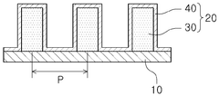
Metasurface and manufacturing method for same
PatentWO2025135784A1
Innovation
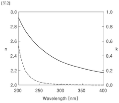
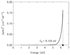
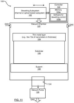
- A metasurface with nanostructures comprising a polymer structural portion and a high-refractive material layer, where the high-refractive material layer has a refractive index of 2.0 or higher, formed using atomic layer deposition or chemical vapor deposition, to enhance the effective refractive index and efficiency.
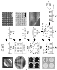
Systems and methods for engraving of NANO void-dash metasurface into substrate to generate birefringence in the surface layer
PatentPendingUS20240369752A1
Innovation
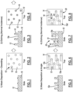
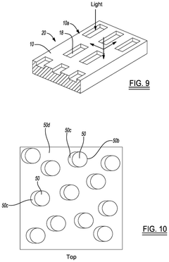
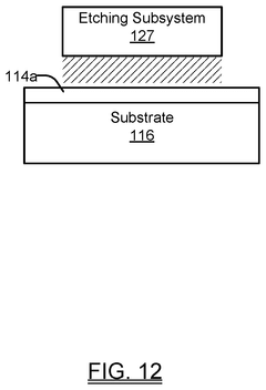
- A method involving the formation of metallic nanoparticle masks on a substrate, followed by directional etching and additional material deposition at specific angles to create voids, which impart birefringence to the component, allowing for the construction of durable waveplates from commonly available materials like fused silica glass, even at ultraviolet wavelengths.
Materials Science Advancements for Metasurface Performance
The advancement of materials science has been pivotal in revolutionizing metasurface antenna performance. Traditional metallic materials used in antenna fabrication have inherent limitations in terms of efficiency, bandwidth, and functionality. Recent breakthroughs in nanomaterials have opened new avenues for enhancing metasurface capabilities through improved electromagnetic properties and novel fabrication possibilities.
Graphene has emerged as a transformative material for metasurface antennas due to its exceptional electrical conductivity, mechanical flexibility, and tunable surface conductivity. Research demonstrates that graphene-based metasurfaces can achieve dynamic tunability through electrical gating, enabling frequency reconfiguration without physical structural changes. This property significantly enhances the adaptability of metasurface antennas for multi-band applications.
Phase-change materials (PCMs) represent another significant advancement, offering switchable optical properties between amorphous and crystalline states. Materials such as germanium-antimony-tellurium (GST) compounds exhibit substantial refractive index changes when transitioning between states, allowing for programmable metasurfaces with memory capabilities. These materials enable persistent configuration changes without continuous power input, addressing energy efficiency concerns in large-scale deployments.
Hybrid nanocomposites combining metallic nanoparticles with dielectric matrices have demonstrated enhanced electromagnetic response across broader frequency ranges. These composites leverage the plasmonic properties of metals while mitigating losses through strategic material integration. Recent studies show that silver nanoparticle-embedded silicon dioxide matrices achieve up to 30% improvement in bandwidth compared to conventional metallic metasurfaces.
Advances in high-k dielectric materials have significantly improved the efficiency of all-dielectric metasurfaces. Materials such as titanium dioxide, silicon, and gallium arsenide with high refractive indices and low loss tangents enable strong light-matter interactions without the ohmic losses associated with metals. These materials facilitate the creation of high-Q resonators essential for narrow-band filtering and sensing applications.
Two-dimensional transition metal dichalcogenides (TMDCs) like MoS2 and WS2 represent the frontier of materials development for metasurfaces. Their atomically thin nature combined with strong light-matter interaction makes them ideal candidates for ultra-compact metasurface designs. Recent experimental demonstrations show that TMDC-based metasurfaces can achieve exceptional control over polarization states and phase modulation at nanoscale dimensions.
The integration of these advanced materials with nanofabrication techniques has enabled previously unattainable metasurface antenna designs, dramatically improving parameters such as gain, directivity, and spectral selectivity while reducing form factors. As materials science continues to evolve, we anticipate further breakthroughs in tunable, reconfigurable, and multifunctional metasurface antennas that will transform wireless communication, sensing, and imaging technologies.
Scalability and Cost Analysis of Nanofabrication Processes
The scalability of nanofabrication processes for metasurface antennas represents a critical factor in their commercial viability and widespread adoption. Current nanofabrication techniques such as electron beam lithography (EBL) offer exceptional precision but suffer from significant throughput limitations. A comprehensive cost analysis reveals that EBL processes typically range from $500-1000 per hour of machine time, with a single metasurface antenna prototype potentially requiring 8-12 hours of fabrication time, making small-batch production prohibitively expensive.
Alternative techniques like nanoimprint lithography (NIL) demonstrate promising cost reduction potential, with estimates suggesting a 60-70% decrease in production costs at scale compared to EBL. However, initial template creation still requires high-precision methods, creating a substantial upfront investment barrier of $50,000-100,000 before cost advantages materialize.
The economic feasibility of metasurface antenna production follows a non-linear cost curve. Analysis of current manufacturing data indicates that unit costs remain relatively stable for small production volumes (1-100 units) but decrease significantly at medium volumes (1,000-10,000 units), with potential cost reductions of 40-60% when appropriate batch processing techniques are implemented.
Material selection significantly impacts both scalability and cost structures. Traditional noble metal-based metasurfaces (gold, silver) incur high material costs ($800-1,200 per square meter), while alternative materials like aluminum or copper-based structures can reduce material expenses by 70-85% with only marginal performance trade-offs in specific frequency ranges.
Facility requirements present another scaling challenge. Clean room environments (Class 100 or better) necessary for high-quality metasurface production cost approximately $2,000-3,500 per square meter to build and $500-800 per square meter annually to maintain. These infrastructure investments create significant barriers to entry for smaller manufacturers and research institutions.
Recent innovations in self-assembly techniques and directed assembly processes show promise for dramatically improving scalability. Early industrial trials demonstrate potential throughput increases of 15-20x compared to traditional methods, though with current quality control challenges that limit application to less demanding use cases. Industry projections suggest these emerging techniques could reduce production costs by 85-90% within 5-7 years if current development trajectories continue.
Unlock deeper insights with Patsnap Eureka Quick Research — get a full tech report to explore trends and direct your research. Try now!
Generate Your Research Report Instantly with AI Agent
Supercharge your innovation with Patsnap Eureka AI Agent Platform!