

Power-junction-type field effect transistor and manufacturing method thereof
A technology of field effect transistors and junctions, which is applied in semiconductor/solid-state device manufacturing, electrical components, circuits, etc., can solve the problems of limited pinch-off voltage, current drive ability, etc.
Patent Information
- Authority / Receiving Office
- CN · China
- Current Assignee / Owner
- Publication Date
- 2015-09-09
Smart Images
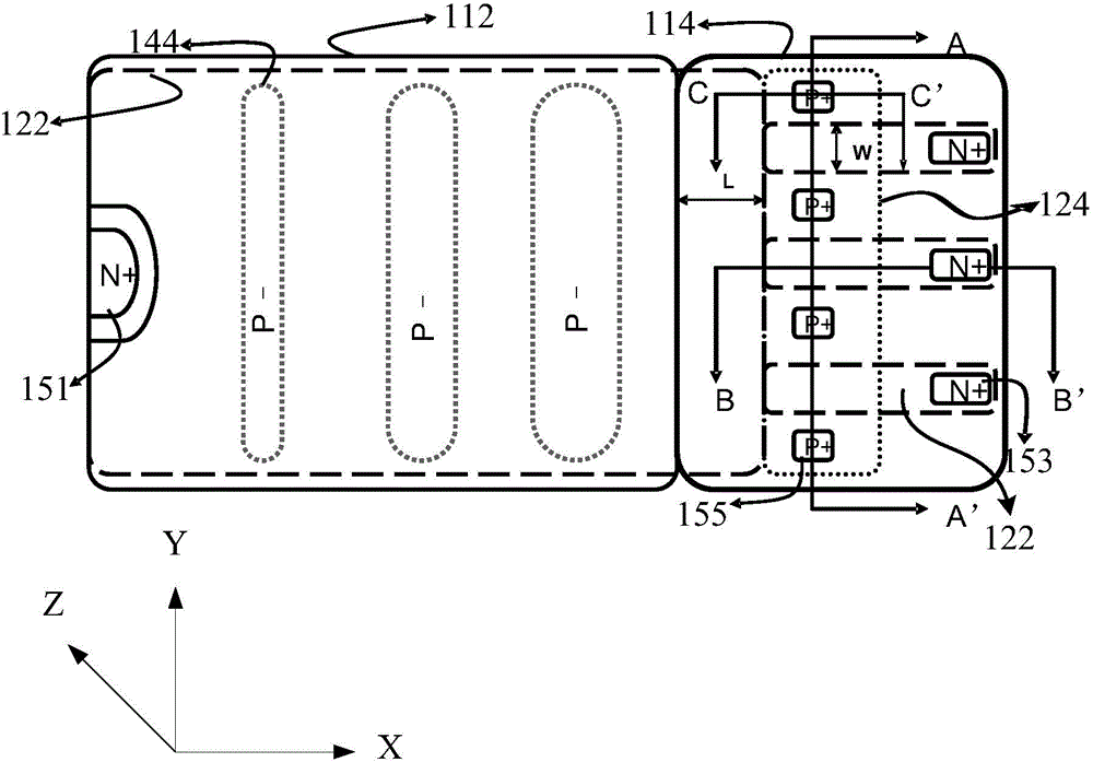
Figure 1 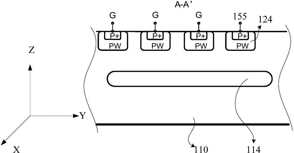
Figure 2 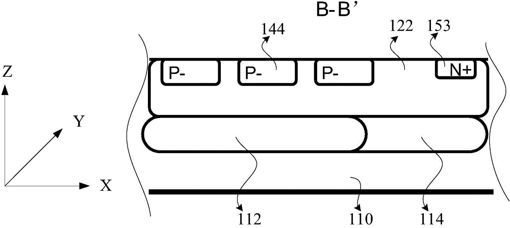
Figure 3
Abstract
Description
technical field
[0001] The invention relates to a semiconductor device, in particular to a power junction field effect transistor, a circular power junction field effect transistor, and a manufacturing method of the power junction field effect transistor. Background technique
[0002] Junction Field Effect Transistor (JFET) is a very important type of device. Using JFET can easily build a start-up module and a constant current source module. For JFET, its pinch-off voltage is one of the critical parameters.
[0003] The pinch-off voltage of the device depends on the depletion of carriers, because when the pinch-off point is balanced, the carriers in the depletion layer are mainly provided by the well region, which is generally formed by separate ion implantation and It is realized by pushing the well, so it is easier to control the doping concentration and depth of the well region by controlling the parameters such as the energy and dose of the ion implantation and the temp...
Examples
Embodiment Construction
[0031] In order to make the objects, features and advantages of the present invention more comprehensible, specific implementations of the present invention will be described in detail below in conjunction with the accompanying drawings.
[0032] The power junction field effect transistor includes a substrate of the first doping type, a buried layer region located above the substrate along the Z-axis direction in a three-dimensional coordinate system, a well region located above the buried layer region along the Z-axis direction, and a second doped The source of the heterotype, the drain of the second doping type, the gate of the first doping type, and the junction region of the first doping type; the source, the drain, the gate and the junction region are located in the well region.
[0033] figure 1 It is a top view structure diagram of a power junction field effect transistor in an embodiment, figure 2 is along figure 1 A cross-sectional view of line A-A' in image 3 is...