
Liquid-crystal device and production thereof
A technology for a liquid crystal display and a manufacturing method, which is applied to static indicators, photolithographic process exposure devices, instruments, etc., can solve problems such as uneven cell gaps and uneven panel chromaticity, so as to reduce production costs, simplify processes, and increase The effect of the operating range
Patent Information
- Authority / Receiving Office
- CN · China
- Patent Type
- Patents(China)
- Current Assignee / Owner
- Publication Date
- 2009-05-20
- Estimated Expiration
- Not applicable · inactive patent
Smart Images
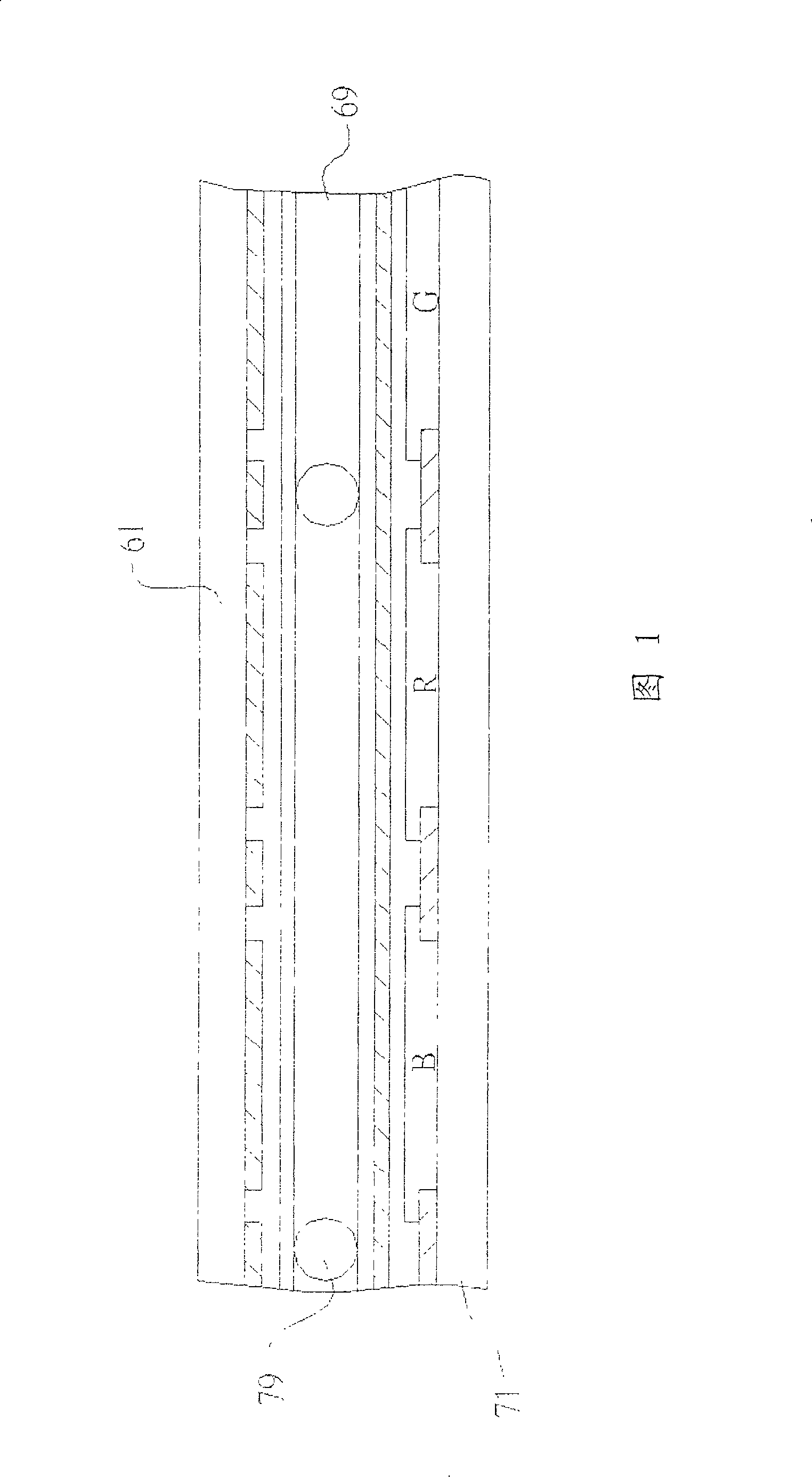
Figure 1 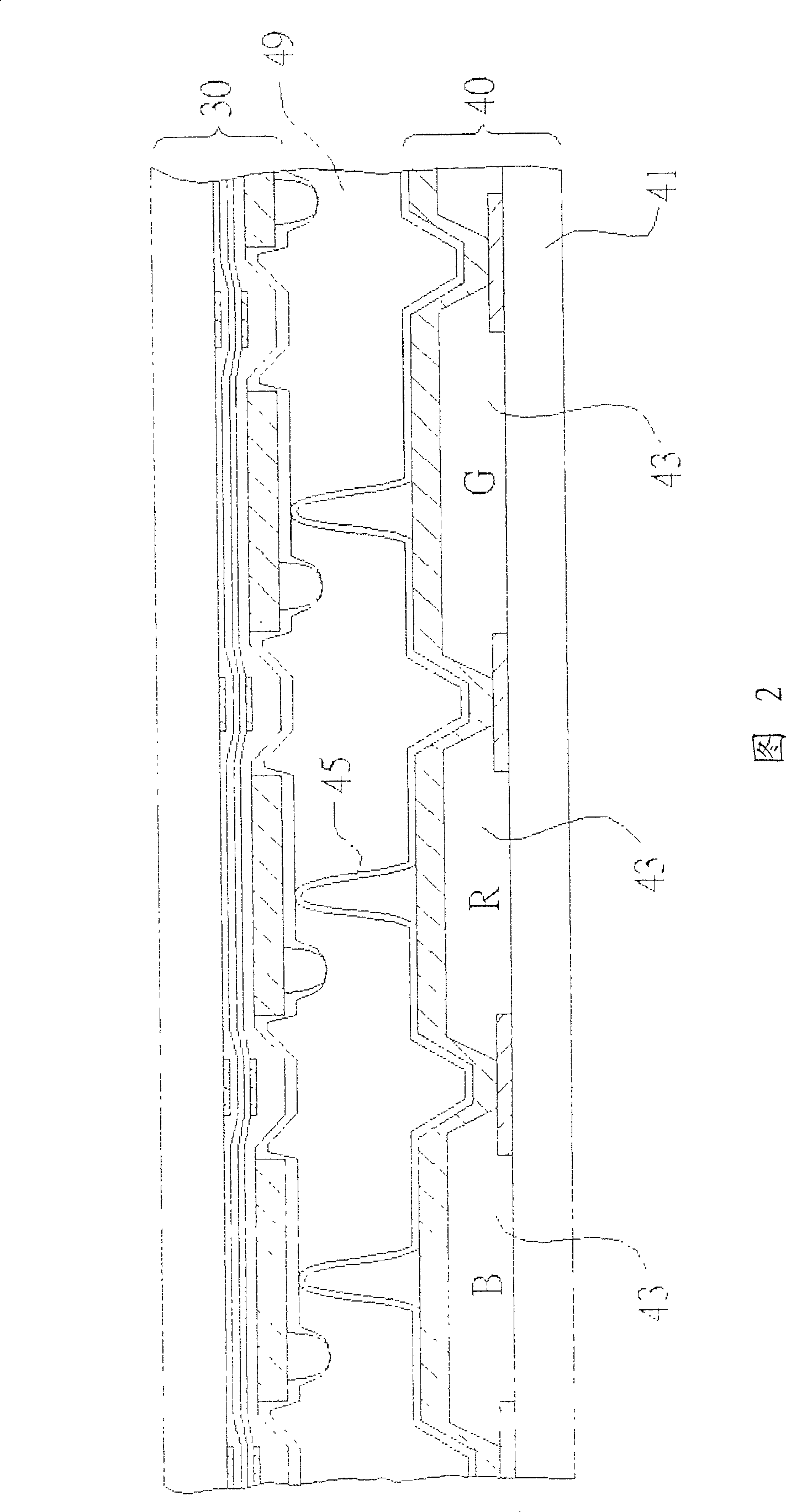
Figure 2 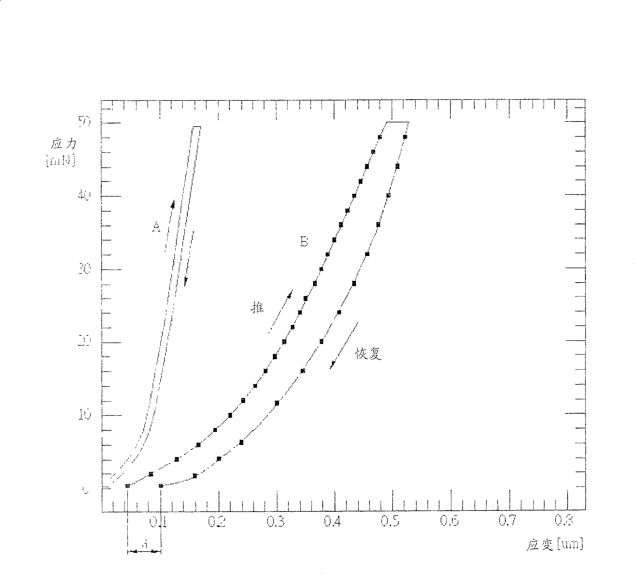
Figure 3
Abstract
Description
technical field
[0001] The invention relates to a structure of a display device and a manufacturing method thereof, in particular to a structure of a liquid crystal display device and a manufacturing method thereof. Background technique
[0002] A liquid crystal display device typically includes a pair of substrates maintained in a spaced-apart and parallel relationship to each other. The space between the substrates is generally called a liquid crystal cell gap or a cell gap. A liquid crystal material is interposed between the two substrates, located in the cell gap, and can change its optical characteristics in response to an external electronic signal.
[0003] A plurality of electrodes are placed on the inner surface of the substrate for controlling the electronic signal and acting on the liquid crystal material. Some types of liquid crystal display devices have an arrangement of electrodes capable of producing a predetermined set of characters or symbols, while other ...
Examples
Embodiment Construction
[0104] 4a, 4b and 4c, which shows a gap sub-substrate according to an embodiment of the present invention, such as a color filter (Color Filter; hereinafter referred to as CF) substrate 100, for a thin film transistor (Thin Film Transistor; TFT) liquid crystal display (Liquid Crystal Display; LCD) device.
[0105] As shown in FIG. 4 a , it shows that a pixel (pixel) on the CF substrate 100 includes three sub-pixels (sub-pixel). The pixels correspond to thin film transistors on the TFT substrate (not shown in the figure) of the LCD device. Now for further reference Figure 4b and 4c , which is a cross-sectional view of the CF substrate 100 along section lines 4b-4b and 4c-4c in FIG. 4a. The CF substrate 100 has a transparent substrate, such as a glass substrate 120 . A black matrix 150 is generally made of metal, such as chromium (Cr) or chromium oxide (CrOx) in thin film form, or black resin, and is covered on the glass substrate 120, and part of the glass substrate 120 is...