
Phase change storage device based on antimony telluride composite phase change material and preparation method thereof
A composite phase-change material and phase-change storage technology, which is applied in the field of phase-change storage devices and its preparation, can solve the problems of unfavorable memory data retention, no reporting of doping substances, and non-practicability, etc., to improve data retention capabilities , Reduce the RESET operating current, the effect of increasing the crystal resistivity
Patent Information
- Authority / Receiving Office
- CN · China
- Patent Type
- Patents(China)
- Current Assignee / Owner
- Publication Date
- 2012-09-19
- Estimated Expiration
- Not applicable · inactive patent
Smart Images
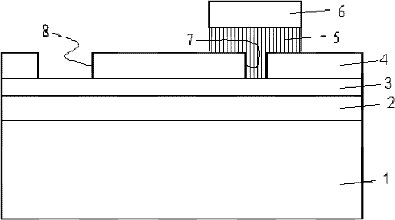
Figure 1 
Figure 2 
Figure 3
Abstract
Description
technical field
[0001] The invention relates to a device in the field of computer technology, in particular to a phase change storage device based on an antimony telluride composite phase change material and a preparation method thereof. Background technique
[0002] Phase change memory is a new semiconductor non-volatile storage device. Compared with the existing dynamic random access memory (DRAM), it has the characteristics of non-volatility, that is, when it is set to any state, even if the power is cut off, the storage unit remains is the resistance value for this state, unless the state of the memory cell is reset. Compared with the existing non-volatile memory FLASH (flash memory), it can work in a smaller device size, has faster erasing speed, more erasing times, better data retention, and has no need Rewriting, compatibility with CMOS (complementary metal oxide semiconductor) technology and radiation resistance, etc., so phase change memory is considered to be a ne...
Examples
Embodiment
[0044] like figure 1 As shown, the phase change memory device based on the antimony telluride composite phase change material involved in this embodiment includes: a substrate 1, a lower electrode 2, a heat generating electrode layer 3, an insulating layer 4, a phase change material layer 5 and an upper electrode 6 , wherein: the lower electrode 2 is arranged on the substrate 1, the heat generating electrode layer 3 is arranged on the lower electrode 2, the insulating layer 4 is arranged on the heat generating electrode layer 3, a fine hole 7 is arranged in the insulating layer 4, and the phase change material layer 5 is filled in the pores 7 of the insulating layer 4 and is in contact with the heat generating electrode layer 3 , and the upper electrode 6 is disposed on the phase change material layer 5 .
[0045] The heat generating electrode layer 3 is provided with a lower electrode outlet 8 communicating with the lower electrode 6 .
[0046] The substrate 1 is a silicon s...