
P-N junction diode structure of MOS (metal-oxide semiconductor)
An oxide semiconductor, P-N technology, applied in the direction of semiconductor devices, transistors, electrical components, etc., can solve the problems of high forward voltage drop and low forward voltage drop, and achieve low forward voltage drop , low leakage current, small reverse bias leakage current effect
Patent Information
- Authority / Receiving Office
- CN · China
- Patent Type
- Patents(China)
- Current Assignee / Owner
- Publication Date
- 2015-05-06
Smart Images
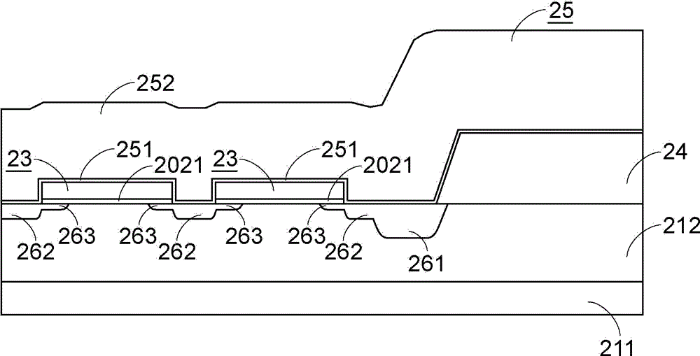
Figure 1 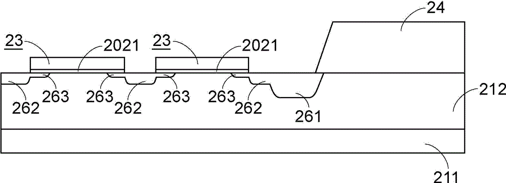
Figure 2 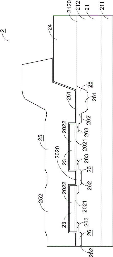
Figure 3
Abstract
Description
[0001] The present invention is a divisional application. The filing date of the original application is: April 2, 2009; the original application number is: 200910132565.4; the original invention creation name is: metal oxide semiconductor P-N junction diode structure and its manufacturing method. technical field
[0002] The invention relates to a metal oxide semiconductor P-N junction diode structure and a manufacturing method thereof, in particular to a diode with lower leakage current and lower forward conduction voltage drop (V F ), a metal oxide semiconductor P-N junction diode structure with high reverse withstand voltage value and low reverse recovery time characteristics. Background technique
[0003] Schottky diode is a unipolar element with electrons as carriers, and its characteristics are fast speed and forward conduction voltage drop value (V F ) is low, but the reverse bias leakage current is relatively large (related to the Schottky barrier value caused by th...
Examples
Embodiment Construction
[0033] See Figure 7, which is a schematic diagram of a preferred embodiment of a metal-oxide-semiconductor P-N junction diode structure developed by the present invention to improve the shortcomings of known technical means. From the figure, we can clearly see that the structure of the metal oxide semiconductor P-N junction diode 2 mainly includes a substrate 21, a trench structure 22, a gate structure 23, a sidewall structure 24, a metal layer 25 and an ion implantation region. 26, wherein the substrate 21 is composed of a highly doped N-type silicon substrate (N+ silicon substrate) 211 and a low doped N-type epitaxial layer (N- epitaxial layer) 212, and the trench structure 22 is formed on the substrate 21, the gate structure 23 is formed in the trench structure 22 and protrudes from the surface 2120 of the low-doped N-type epitaxial layer 212, and the sidewall structure 24 protrudes from the surface of the substrate 21 and is located on the gate On the side of the structu...