
LDMOS ESD(Laterally Diffused Metal Oxide Semiconductor Electro-Static Discharge) structure
A source and drain technology, applied in electrical components, circuits, semiconductor devices, etc., can solve the problems of increasing IC design cost and device size, and achieve enhanced antistatic capability, increased effective channel length, and effective channel length. The effect of increasing the channel resistance
Patent Information
- Authority / Receiving Office
- CN · China
- Patent Type
- Applications(China)
- Current Assignee / Owner
- Publication Date
- 2012-03-14
Smart Images
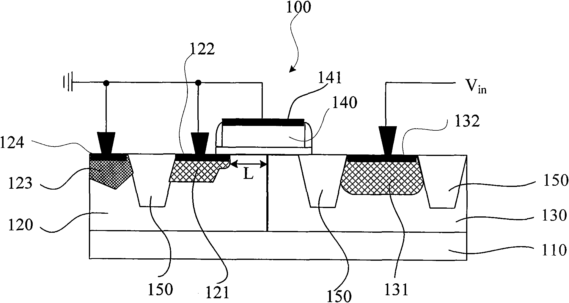
Figure 1 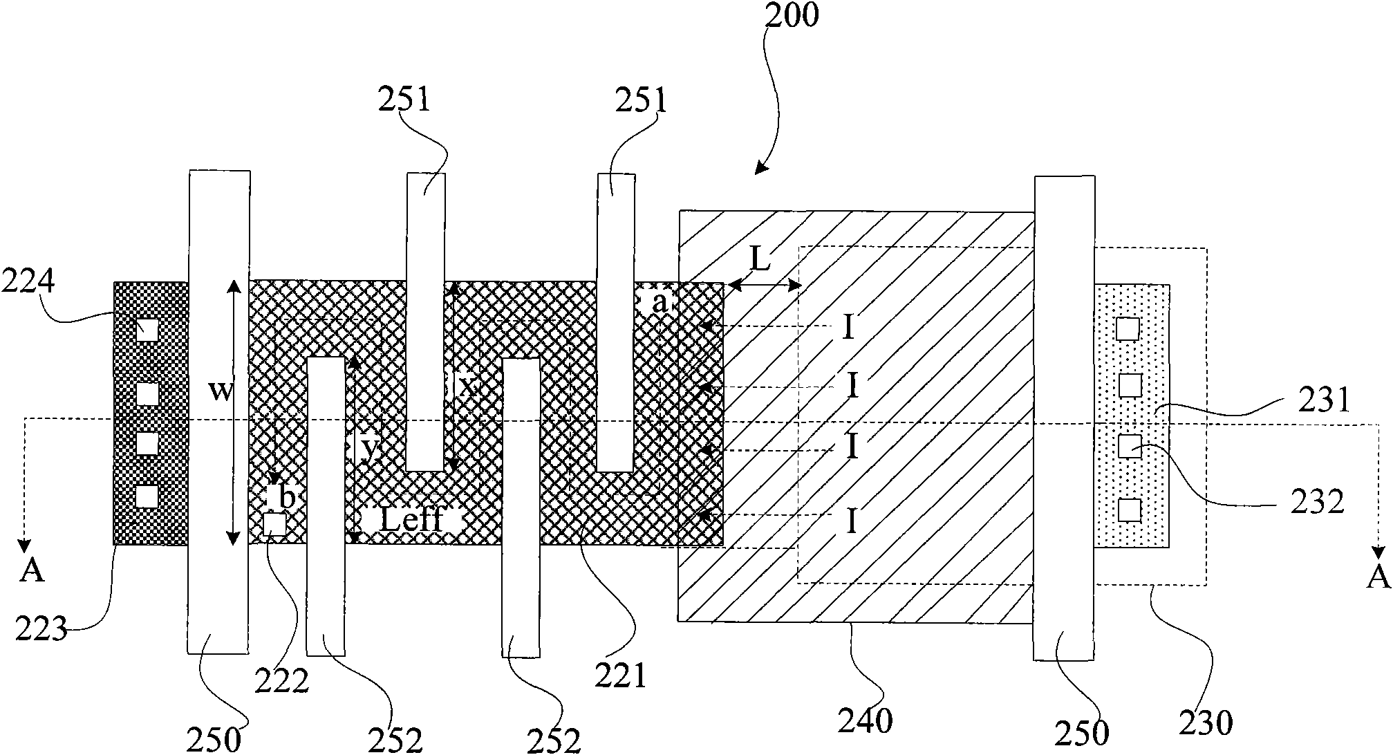
Figure 2 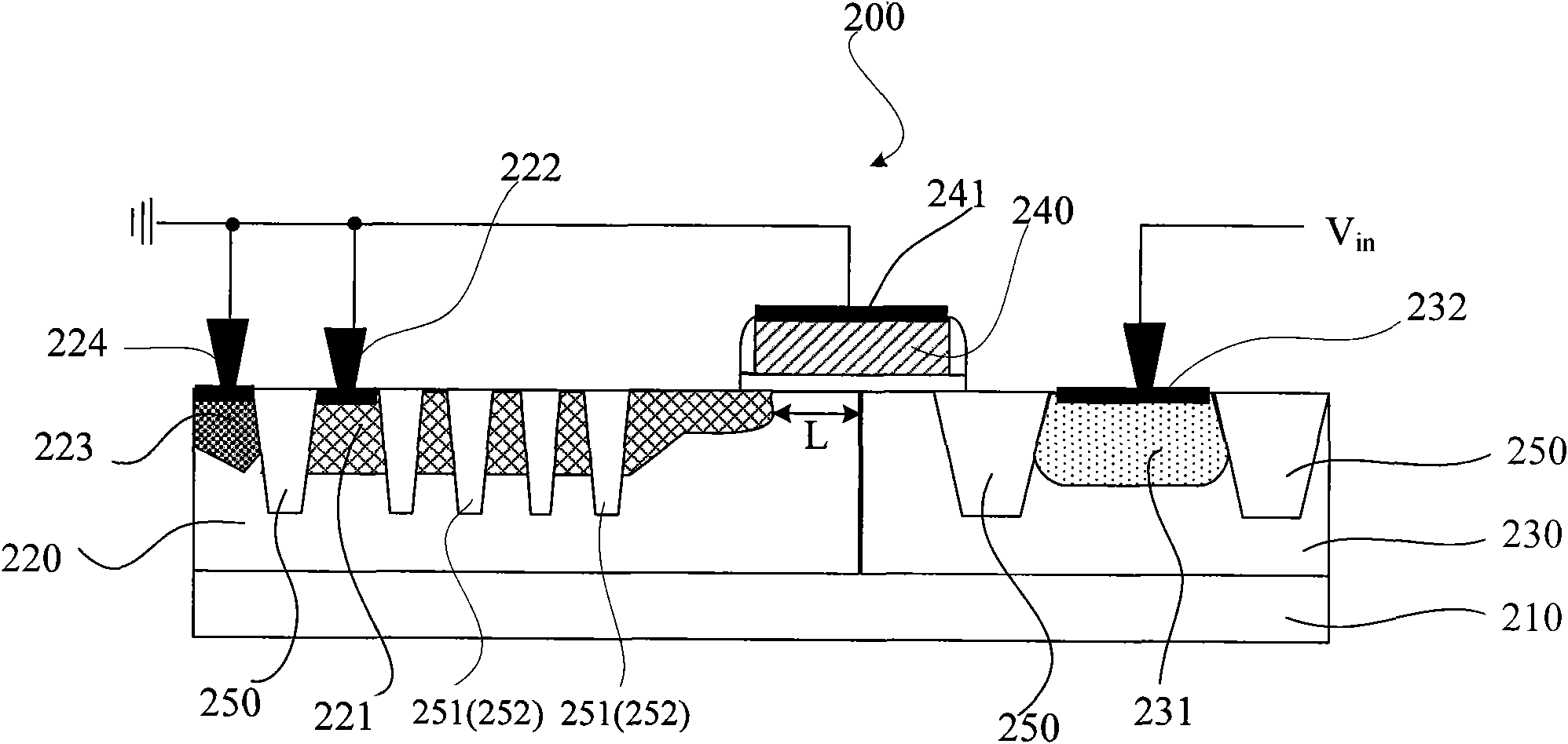
Figure 3
Abstract
Description
technical field
[0001] The invention relates to the technical field of integrated circuits, in particular to an LDMOS ESD structure which can effectively reduce device size. Background technique
[0002] As the level of integrated circuit manufacturing technology enters the deep submicron era of integrated circuit line width, the feature size of CMOS technology continues to shrink, and the ability of transistors to withstand high voltage and high current continues to decrease. Deep submicron CMOS integrated circuits are more susceptible to electrostatic shock failure, resulting in a decrease in product reliability.
[0003] Static electricity is ubiquitous in the process of chip manufacturing, packaging, testing and use. The accumulated static charge is released in nanoseconds to microseconds with a current of several amperes or tens of amperes. The instantaneous power is as high as hundreds of kilowatts, and the discharge energy It can reach millijoules, and the destructio...
Examples
Embodiment Construction
[0033] The LDMOS ESD structure proposed by the present invention will be further described in detail below in conjunction with the drawings and specific embodiments. Advantages and features of the present invention will be apparent from the following description and claims. It should be noted that the drawings are all in a very simplified form and use imprecise ratios, which are only used to facilitate and clearly assist the purpose of illustrating the embodiments of the present invention.
[0034] The core idea of the present invention is to provide an LDMOS ESD structure, the LDMOS ESD structure is provided with an interdigitated STI structure in the source region, so that the flow direction of the electrostatic discharge current of the LDMOS ESD is in a square wave shape, thereby Without increasing the actual channel length, the effective channel length is increased, the effective channel resistance is increased, the holding voltage is further increased, and the antistati...