
Manufacturing method of trench isolation structure
A technology of isolation structure and manufacturing method, applied in semiconductor/solid-state device manufacturing, electrical components, circuits, etc., can solve the problems of deteriorating the characteristics and reliability of memory components, and achieve the effect of optimal component characteristics and reliability
Patent Information
- Authority / Receiving Office
- CN · China
- Patent Type
- Applications(China)
- Current Assignee / Owner
- Publication Date
- 2012-08-29
Smart Images
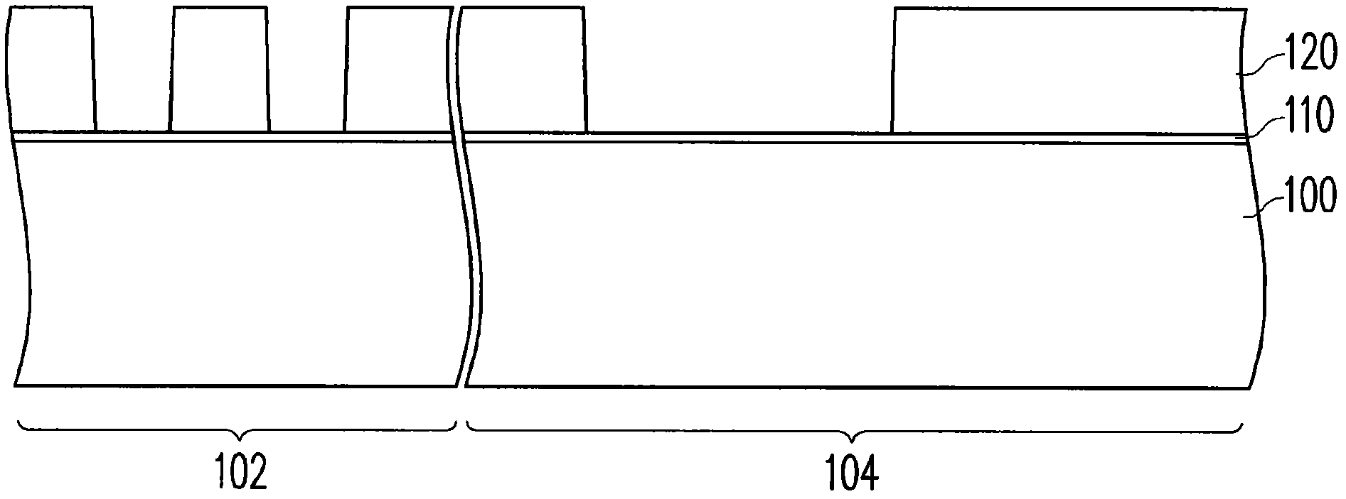
Figure 1 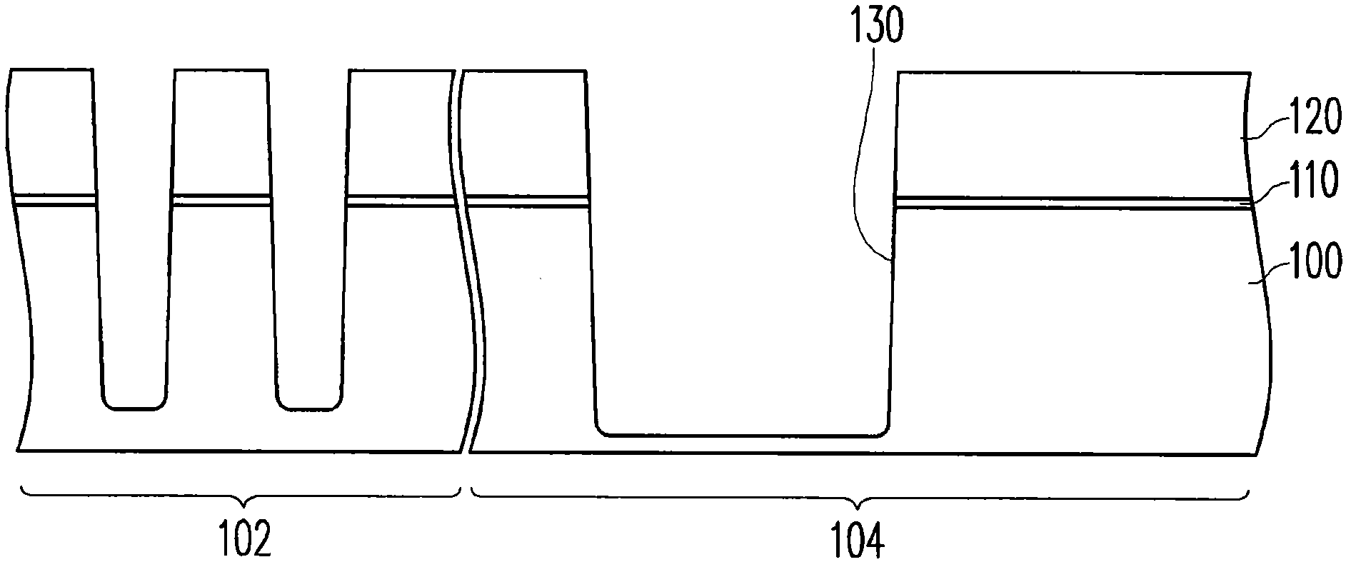
Figure 2 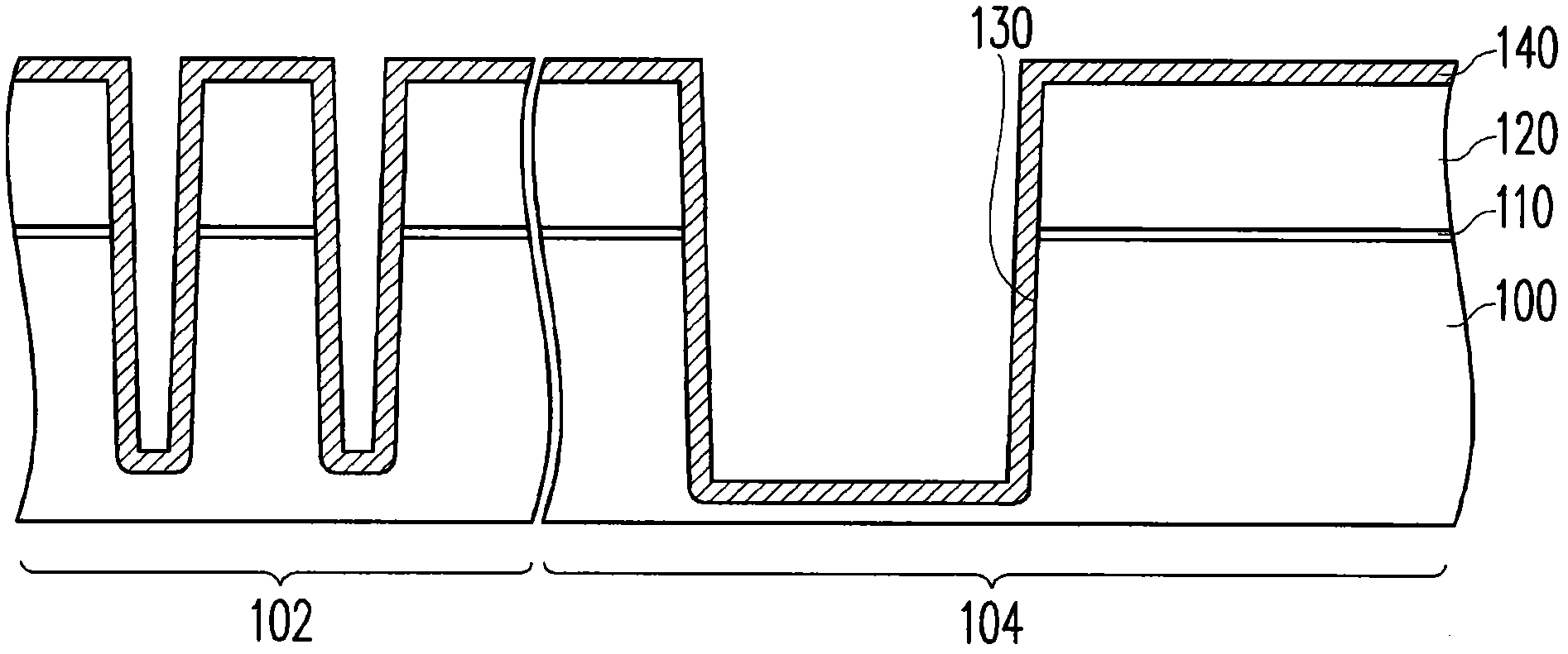
Figure 3
Abstract
Description
technical field
[0001] The invention relates to a method for manufacturing an isolation structure, and in particular to a method for manufacturing a shallow trench isolation structure. Background technique
[0002] With the advancement of semiconductor technology, the size of components is also continuously reduced. Therefore, in order to prevent the occurrence of short circuit between adjacent components, the isolation between components becomes very important. The more commonly used method today is the Shallow Trench Isolation (STI) process.
[0003] Generally, the formation of the STI structure includes forming a pad oxide layer and a patterned mask layer on the substrate, and then removing part of the substrate by using the patterned mask layer as a mask to form shallow trenches in the substrate. . Then, an insulating material is filled in the shallow trench to form a shallow trench isolation structure, and then the pad oxide layer and the patterned mask layer are rem...
Examples
Embodiment Construction
[0040] Generally speaking, since the peripheral area is usually used to form high-voltage elements and low-voltage elements, before the formation of the gate oxide layer, the peripheral area usually bears more wet etching than the memory cell area, and the high-voltage gate oxide layer in the peripheral area usually bears more wet etching. Thickness reduction is difficult or limited, so the corner thinning problem of the high-voltage gate oxide layer is also more serious in the peripheral region, and the low-voltage gate oxide layer may even grow in the recess. As a result, the device characteristics and reliability of the memory device are degraded. Therefore, the present invention forms the shallow trench isolation structure according to the characteristics of the peripheral area of the memory element and the memory cell area, so as to avoid the angle thinning of the tunnel oxide layer and the gate oxide layer formed on the edge of the shallow trench isolation structure sub...