
A trench Schottky semiconductor device with multiple insulating layer isolation and its preparation method
A semiconductor and insulating layer technology, which is applied in the field of trench Schottky semiconductor devices, can solve the problems of multiple times, high on-resistance and reverse leakage current characteristics, so as to increase the doping concentration, reduce the forward conduction resistance, Effect of Improving Reverse Voltage Blocking Characteristics
Patent Information
- Authority / Receiving Office
- CN · China
- Patent Type
- Patents(China)
- Current Assignee / Owner
- Publication Date
- 2016-08-03
Smart Images
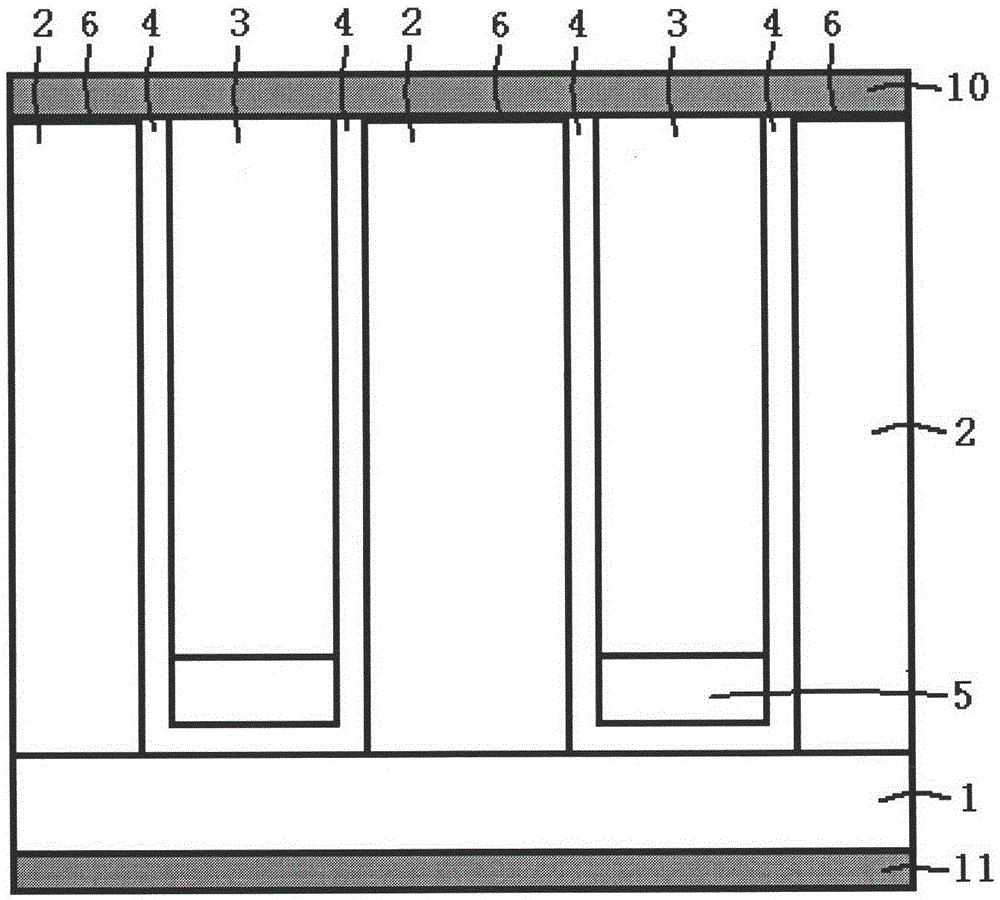
Figure 1 
Figure 2 
Figure 3
Abstract
Description
Technical field
[0001] The invention relates to a trench Schottky semiconductor device with a variety of insulating layer isolations, and the invention also relates to a method for preparing a trench Schottky semiconductor device with a variety of insulating layer isolations. Background technique
[0002] Power semiconductor devices are widely used in power management and power applications. Especially semiconductor devices involving trench structures have become an important trend in device development. Schottky devices have the advantages of low forward turn-on voltage and fast turn-on and turn-off speed. At the same time, Schottky devices also have the disadvantages of large reverse leakage current and cannot be used in high-voltage environments.
[0003] Schottky diodes can be manufactured through a variety of different layout techniques, the most commonly used planar layout. A typical trench layout is shown in BJBaliga's Patent No. 5612567. The traditional trench-type Schott...
Examples
Embodiment 1
[0035] figure 1 It is a trench Schottky semiconductor device with a variety of insulating layer isolations of the present invention, and the following combination figure 1 The semiconductor device of the present invention will be described in detail.
[0036] A trench Schottky semiconductor device with multiple insulating layers isolation, including: a substrate layer 1, which is a semiconductor silicon material of N conductivity type, and the doping concentration of phosphorus atoms is 1E19 / CM 3 , On the lower surface of the substrate layer 1, the electrode is drawn through the lower surface metal layer 11; the N-type semiconductor silicon material 2, located on the substrate layer 1, is a semiconductor silicon material of N conductivity type, and the doping concentration of phosphorus atoms is 1E16 / CM 3 ; P-type semiconductor polysilicon material 3, located on the upper part of the substrate layer 1, is a semiconductor polysilicon material of P conductivity type, and the doping co...