
Fabrication method of gallium nitride laser cavity surface
A manufacturing method and laser technology, applied to lasers, laser components, semiconductor lasers, etc., can solve the problems of increased laser threshold density, uneven bombardment, and inability to generate resonance, so as to improve reflectivity, simplify the process, and eliminate damage Effect
Patent Information
- Authority / Receiving Office
- CN · China
- Current Assignee / Owner
- Publication Date
- 2014-04-02
Smart Images
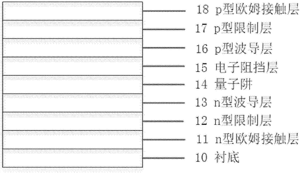
Figure 1 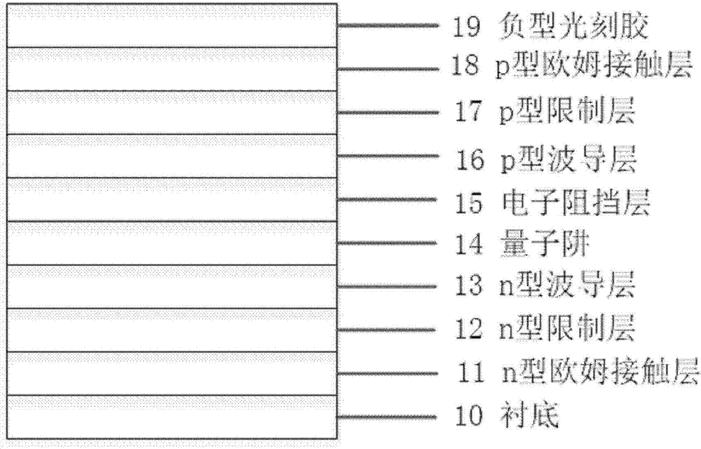
Figure 2 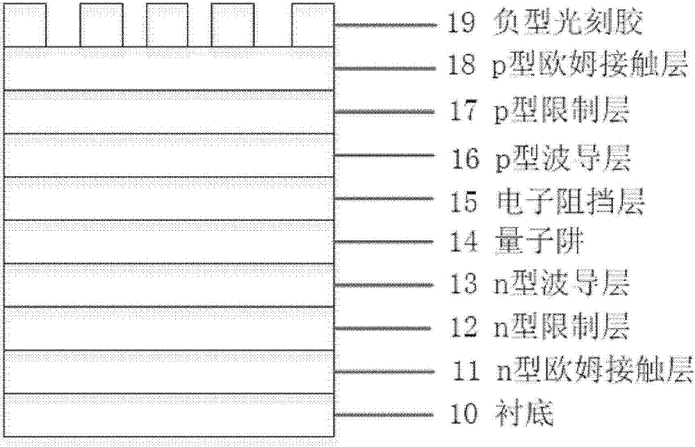
Figure 3
Abstract
Description
technical field
[0001] The invention belongs to the technical field of semiconductors, in particular to a method for manufacturing a gallium nitride material laser cavity surface. Background technique
[0002] Gallium nitride laser With the improvement of gallium nitride (GaN) material crystal quality, optimization of process conditions and improvement of substrate conditions, related technologies have been vigorously developed. For more than ten years, people have made quite remarkable achievements in this field. Advances in epitaxial growth techniques, low-defect substrate materials, and mature device designs have made high-performance GaN-based blue lasers a reality. These products have been used as key components in next-generation DVD playback systems, such as Blu-ray Discs. In addition, these lasers are also suitable for fields such as projection display, high-precision printing and optical sensing. With its unique energy band structure, gallium nitride materials ca...
Examples
Embodiment Construction
[0029] In order to make the object, technical solution and advantages of the present invention clearer, the present invention will be further described in detail below in conjunction with specific embodiments and with reference to the accompanying drawings.
[0030] The invention provides a method for manufacturing a cavity surface of a gallium nitride laser, comprising the following steps:
[0031] Step S1: epitaxially growing a gallium nitride laser structure on the substrate to obtain a gallium nitride epitaxial wafer. Such as Figure 1A As shown, the GaN laser structure sequentially includes an n-type ohmic contact layer 11 with a thickness of 2-3um from the substrate 10 side, an n-type confinement layer 12 with a thickness of 500-600nm, and an n-type waveguide layer 13 with a thickness of 80-100nm, quantum well 14 with a thickness of 30-50nm, electron blocking layer 15 with a thickness of 20-35nm, p-type waveguide layer 16 with a thickness of 80-100nm, p-type confinement...