
Packaging structure of pressure sensor and manufacturing method thereof
A pressure sensor and packaging structure technology, which is applied in semiconductor/solid-state device manufacturing, piezoelectric/electrostrictive/magnetostrictive devices, semiconductor devices, etc., can solve the problems of low packaging efficiency and poor reliability, and achieve low packaging resistance , Improve reliability and improve production efficiency
Patent Information
- Authority / Receiving Office
- CN · China
- Patent Type
- Patents(China)
- Current Assignee / Owner
- Publication Date
- 2020-01-07
Smart Images
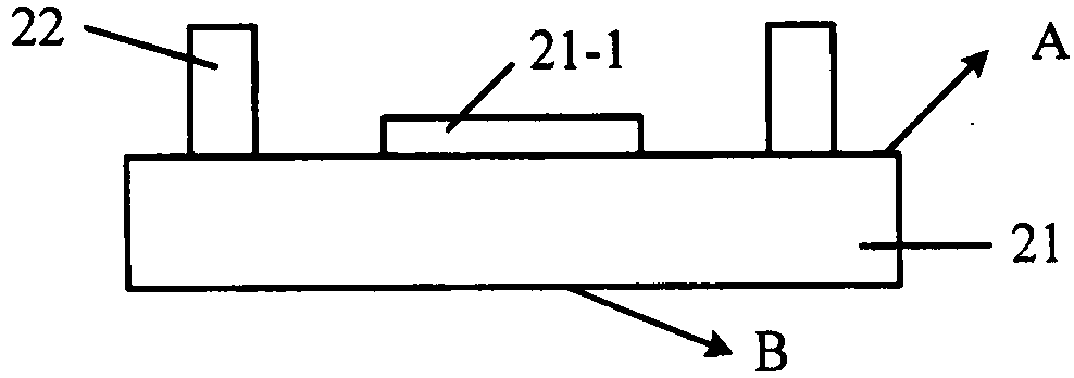
Figure 1 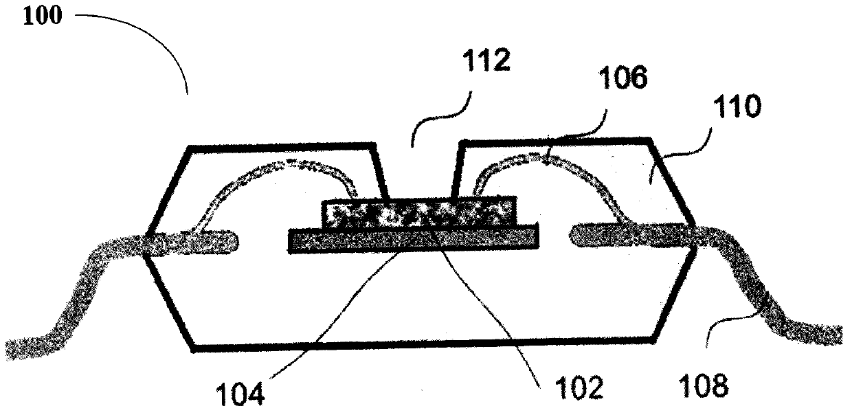
Figure 2 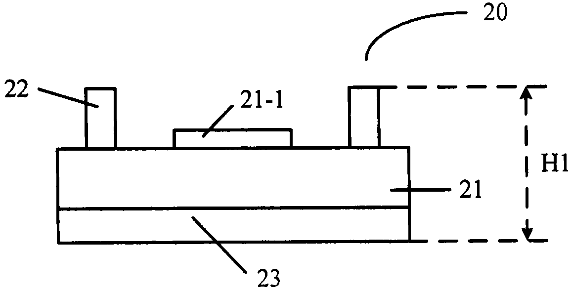
Figure 3
Abstract
Description
technical field
[0001] The invention relates to packaging and manufacturing technology of semiconductor devices, in particular to a packaging structure and packaging method of a pressure sensor. Background technique
[0002] Using the piezoresistive effect of semiconductor silicon, that is, the physical phenomenon that the resistance or resistivity of semiconductor silicon will change significantly when it is subjected to pressure, piezoresistive pressure sensors have been rapidly developed and promoted.
[0003] At the heart of the pressure sensor is a thin-film structure comprising a piezoresistive bridge circuit above a sealed cavity. The pressure-sensitive structure and circuit of the pressure sensor are fabricated above the device, and the film structure with the function of sensing external pressure cannot be inverted, so that the pressure sensor with this structure can only lead out electrical signals through wire bonding.
[0004] figure 1 A schematic diagram 100 s...
Examples
Embodiment Construction
[0045] Hereinafter, the present invention will be described in more detail with reference to the accompanying drawings. In the various figures, identical elements are indicated with similar reference numerals. For the sake of clarity, various parts in the drawings have not been drawn to scale. Also, some well-known parts may not be shown. For the sake of simplicity, the semiconductor structure obtained after several steps can be described in one figure.
[0046] It should be understood that when describing the structure of a device, when a layer or a region is referred to as being "on" or "over" another layer or another region, it may mean being directly on another layer or another region, or Other layers or regions are also included between it and another layer or another region. And, if the device is turned over, the layer, one region, will be "below" or "beneath" the other layer, another region.
[0047] If it is to describe the situation directly on another layer or an...