
Stop band steep dual-stop band ultra wide band (UWB) antenna
A double stopband and stopband technology, applied in the directions of antenna coupling, radiating element structure, etc., can solve the problems of large antenna volume, difficult adjustment of stopband center frequency, unfavorable system integration, etc., achieving low cost, compact structure, and processing. handy effect
Patent Information
- Authority / Receiving Office
- CN · China
- Current Assignee / Owner
- Publication Date
- 2017-06-20
- Estimated Expiration
- Not applicable · inactive patent
Smart Images
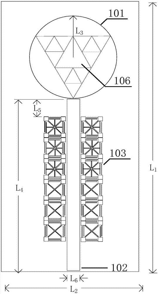
Figure 1 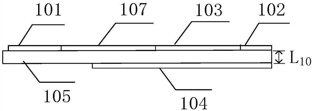
Figure 2 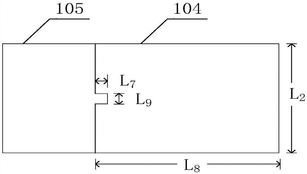
Figure 3
Abstract
Description
technical field
[0001] The invention relates to a UWB band stop antenna, in particular to a dual stop band UWB antenna with steep stop bands, which can suppress the mutual interference problem of a WLAN system (5.15-5.35 GHz). Background technique
[0002] In February 2002, the US Federal Communications Commission (FCC) approved the 3.1-10.6GHz frequency band for commercial communications, so UWB is widely used.
[0003] However, due to the wide frequency band covered by UWB communication, some frequency bands share frequency band resources with other wireless systems, and may interfere with other systems, such as Wimax system (3.2-3.5GHz), WLAN system (5.15-5.35GHz), ( 5.725-5.825GHz) and RFID systems (6.8GHz). How to solve co-channel interference has become an important content of UWB research, so ultra-wideband antennas with stopband characteristics have high practical value.
[0004] In recent years, there have been many design ideas for UWB bandstop antennas, such as ...
Examples
Embodiment Construction
[0023] The present invention designs a UWB antenna with double stop bands and steep stop bands, and the filter can avoid mutual interference with a WLAN system.
[0024] Below in conjunction with accompanying drawing, invention is described in more detail:
[0025] like figure 1 As shown, a dual stopband UWB antenna with steep stopbands of the present invention, the radiation unit (101) on the dielectric substrate, the impedance matching input microstrip line (102), the diamond-shaped etching fractal structure (106), and the cross Type EBG electromagnetic bandgap structure (107), cross-type EBG electromagnetic bandgap structure (103), using copper material.
[0026] An example of the present invention is figure 2 As shown, the dielectric substrate (105) is a GML1000 material with a dielectric constant of 3.2. The dielectric substrate has a thickness of 0.762mm.
[0027] The metal grounding plate (104) under the dielectric substrate is made of copper material.
[0028] li...