
Gate structure and method thereof
A gate dielectric and metal gate technology, applied in the field of gate structure and its formation, can solve problems such as not proving that the existing process is completely satisfactory
Patent Information
- Authority / Receiving Office
- CN · China
- Patent Type
- Patents(China)
- Current Assignee / Owner
- Publication Date
- 2022-06-24
Smart Images
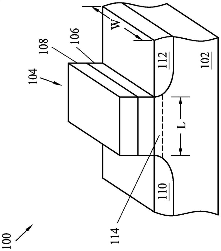
Figure 1 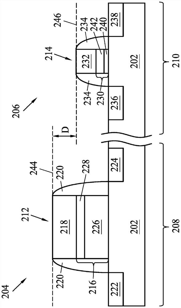
Figure 2 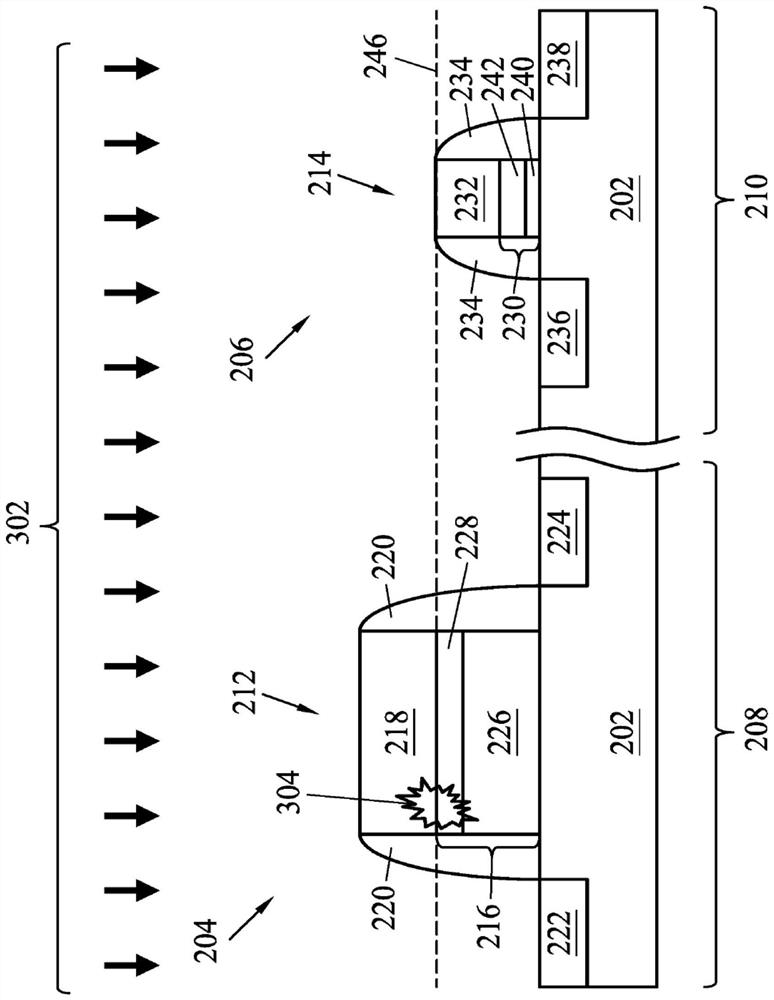
Figure 3
Abstract
Description
technical field
[0001] Embodiments of the present invention relate generally to the field of semiconductors, and more particularly, to gate structures and methods of forming the same. Background technique
[0002] The electronics industry has experienced an ever-increasing demand for smaller and faster electronic devices capable of simultaneously supporting more increasingly complex and sophisticated functions. Accordingly, an ongoing trend in the semiconductor industry is to manufacture integrated circuits (ICs) that are low cost, high performance, and low power consumption. To date, these goals have been largely achieved by scaling down the size of semiconductor ICs (eg, minimum feature size), thereby increasing production efficiency and reducing associated costs. However, this scaling down also creates an increased level of complexity in the semiconductor fabrication process. Accordingly, enabling continued advancement of semiconductor ICs and devices requires similar a...
Examples
Embodiment Construction
[0015] The following disclosure provides many different embodiments or examples for implementing different features of the presented subject matter. Specific examples of components and arrangements are described below to simplify the present disclosure. Of course, these are only examples and are not intended to limit the invention. For example, in the following description, forming the first part over or on the second part may include embodiments in which the first part and the second part are formed in direct contact, and may also include between the first part and the second part Embodiments in which additional components may be formed between, so that the first and second components may not be in direct contact. Furthermore, the present disclosure may repeat reference numerals and / or characters in various instances. This repetition is for the purpose of simplicity and clarity, and does not in itself indicate a relationship between the various embodiments and / or configurat...