
Vector synthesis phase shifter and vector synthesis phase shifting method
A technology of vector synthesis and phase shifter, applied in phase shifting network, multi-terminal pair network, etc., can solve the problem of high power consumption, achieve the effect of reducing power consumption, improving phase shifting accuracy, and ensuring constant gain
Patent Information
- Authority / Receiving Office
- CN · China
- Current Assignee / Owner
- Publication Date
- 2020-07-03
Smart Images
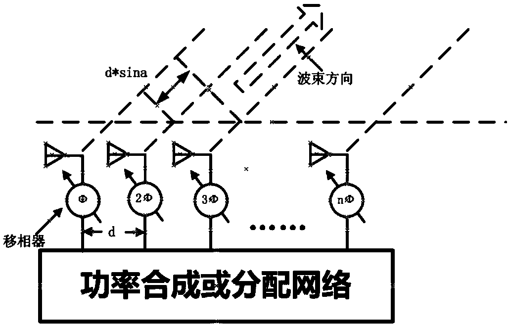
Figure 1 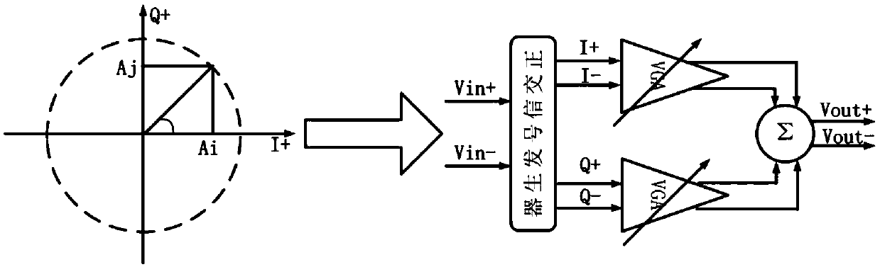
Figure 2 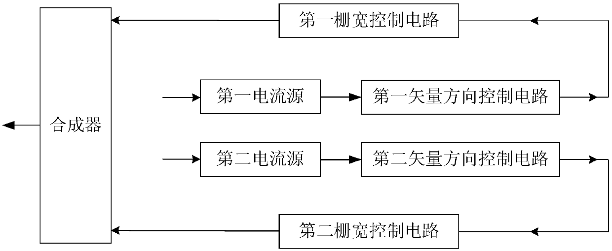
Figure 3
Abstract
Description
technical field
[0001] The invention relates to the field of passive phase shifters, in particular to a vector synthesis phase shifter and a vector synthesis phase shifter method. Background technique
[0002] Phased array technology has the ability of beam forming and beam scanning, which can significantly improve the signal-to-noise ratio and sensitivity of wireless communication systems, and reduce the power and noise requirements of a single channel in the system. Phased array technology is widely used in military for its excellent characteristics. It is widely used in microwave and millimeter wave signal transmission, and has become the key technology of 5G millimeter wave communication. like figure 1 The schematic block diagram of a typical phased array system is shown, and the beam pointing can be changed through the controllable phase difference of different channels, and effective beam synthesis can be performed. Among them, according to the implementation of the ...
Examples
Embodiment 1
[0078] This embodiment illustrates the working process of the vector synthesis phase shifter, as follows:
[0079] like Figure 4 As shown, the present invention not only divides the current source unit of the I channel and the Q channel into the form of a binary array, but also divides the amplifier tube into the form of an M-bit binary array. The power consumption of the entire vector synthesizer can be reduced to the original details as follows:
[0080] Assume that the I current is I 1 , amplifier tube M 1 The width to length ratio is β 1 , the current of Q circuit is I 2 , amplifier tube M 2 The width to length ratio is β 2 , and I 1 ≥I 2 , I 1 +I 2 =C, then there are:
[0081]
[0082] 1. The current I 1 becomes and the transistor M 1 The grid width increases by 2 M , that is, the aspect ratio becomes Then in the case of neglecting the channel adjustment effect, the adjusted transistor M 1 The transconductance of:
[0083]
[0084] It can be s...
Embodiment 2
[0092] The specific implementation method of the present invention is described below with M=2, N=6 as an example. It should be noted that M can be any integer value between 0 and N, and it can be adjusted as needed. The current is C.
[0093] Transistor M 1 structured as Image 6As shown, the corresponding relationship between the phase shift value of the existing scheme (before adjustment) and the grid width, power consumption, and total current is shown in Table 1, and the phase shift value of the scheme (after adjustment) of the present embodiment and the grid width, power consumption The corresponding relationship between power consumption and total current is shown in Table 2. The comparison between adjusted and before adjustment is shown in Table 3. According to the comparison in Table 3, the power consumption optimization is obvious. In addition, the ratio of maximum and minimum current is greatly reduced, which reduces the impact on circuit matching. Require. In ad...