
Display panel and method of making the same
A technology for display panels and manufacturing methods, which is applied in semiconductor/solid-state device manufacturing, semiconductor devices, electrical components, etc., can solve the problems of low service life of OLED display panels, and achieve the effect of increasing service life
Patent Information
- Authority / Receiving Office
- CN · China
- Patent Type
- Patents(China)
- Current Assignee / Owner
- Publication Date
- 2022-07-12
Smart Images
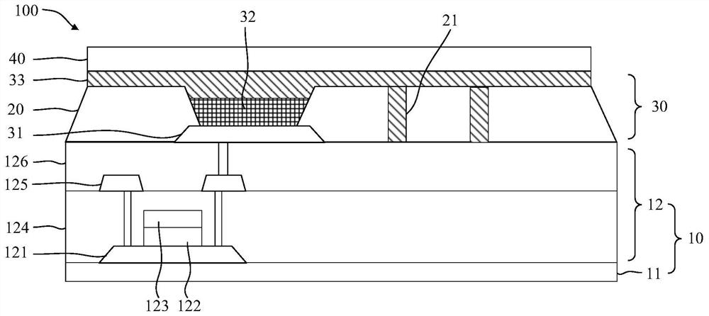
Figure 1 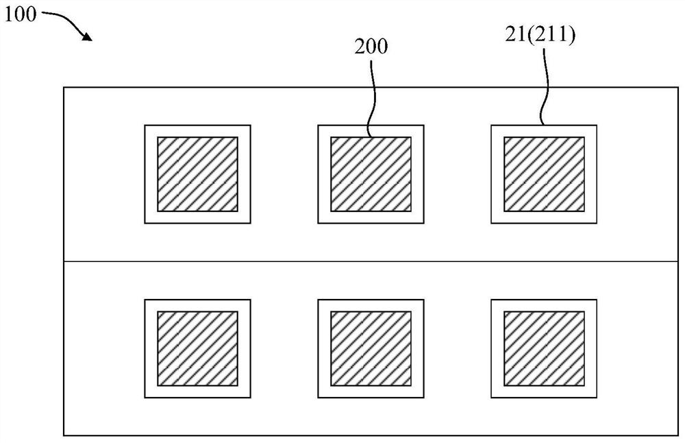
Figure 2 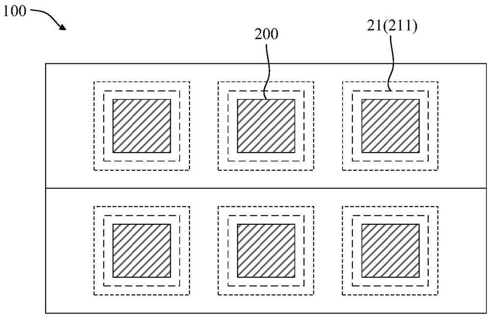
Figure 3
Abstract
Description
technical field
[0001] The present application relates to the field of display, and in particular, to a display panel and a manufacturing method thereof. Background technique
[0002] In display technology, Organic Light-Emitting Diode (OLED) displays have many advantages, such as thinness, active light emission, fast response speed, large viewing angle, wide color gamut, high brightness and low power consumption. The third generation of display technology after the display (LCD).
[0003] In the existing OLED display panel, since the pixel definition layer is generally composed of organic substances, the pixel definition layer has characteristics such as oxygen and hydrophilic properties, that is, there is a large amount of water and oxygen in the pixel definition layer of the existing OLED display panel. With the use of the OLED display panel, water and oxygen in the pixel definition layer may corrode the pixel definition layer, the anode layer or the luminescent material...
Examples
Embodiment Construction
[0042] The technical solutions in the embodiments of the present application will be clearly and completely described below with reference to the accompanying drawings in the embodiments of the present application. Obviously, the described embodiments are only a part of the embodiments of the present application, but not all of the embodiments. Based on the embodiments in this application, all other embodiments obtained by those skilled in the art without creative efforts shall fall within the protection scope of this application.
[0043] In the description of this application, it should be understood that the terms "center", "longitudinal", "lateral", "length", "width", "thickness", "upper", "lower", "front", " rear, left, right, vertical, horizontal, top, bottom, inside, outside, clockwise, counterclockwise, etc., or The positional relationship is based on the orientation or positional relationship shown in the drawings, which is only for the convenience of describing the ...