
Carrier storage type FS-IGBT with low conduction voltage drop and manufacturing method thereof
A carrier storage and low conduction technology, applied in the field of microelectronics, can solve problems such as limiting IGBT performance, and achieve the effects of reducing switching loss, reducing feedback capacitance, and reducing conduction voltage drop
Patent Information
- Authority / Receiving Office
- CN · China
- Patent Type
- Applications(China)
- Current Assignee / Owner
- Publication Date
- 2021-05-04
Smart Images
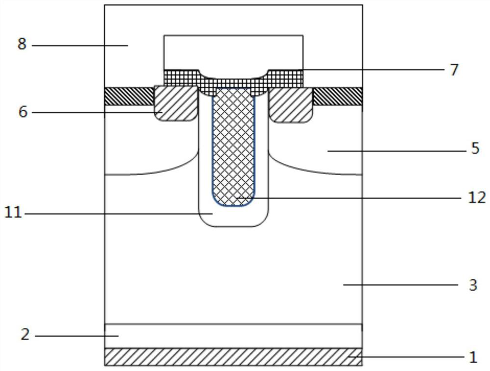
Figure 1 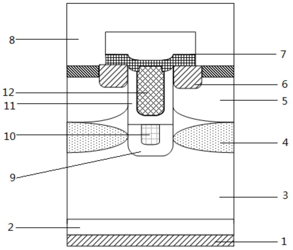
Figure 2
Abstract
Description
Technical field
[0001] The present invention belongs to the field of microelectronics, and is specifically a carrier storage type FS-IGBT and manufacturing method of low-conducting pressure drop.Background technique
[0002] Compared to MOSFETs, the electrical conductive modulation effect of the substrate of the IGBT device can greatly reduce the forward travel pressure drop, the static power loss is small, the higher the voltage, and the performance is more significant. Thus, IGBT accounts great market share in medium and high pressure applications. IGBT mainly has three structures of PT-IGBT, non-pendant NPT-IGBT and field cutoff FS-IGBT, and the main differences between the three are different substrate PN junction structures and different substrate thicknesses. For PT-IGBT and NPT-IGBT, the FS-IGBT has the thinnest thickness, and its forward conduction is significantly decreased, and the structure has been widely used in IGBT products. As the semiconductor wafer is continuously improv...
Examples
Embodiment Construction
[0025]The present invention is further explained in conjunction with specific embodiments.
[0026]A carrier storage type FS-IGBT of a low-conducting passage, which includes a P + type collector 1, N + type buffer layer 2, N-substrate 3, N + type carrier storage layer 4, P-type The body region 5, the N + -type emitter 6, the insulative dielectric layer 7, the emitter metal 8, the shield gate oxide layer 9, the shielding gate polysilicon 10, the gate oxide layer 11 and the gate conductive polysilicon 12;
[0027]The groove is opened downward on the front side of the N-substrate 3, and the shield gate oxide layer 9 is disposed on the lower side of the trench, and the shield gate polysilicon 10 is provided in the shielding gate oxide layer 9, and the upper side of the groove and the upper side of the trench and The gate oxide layer 11 is provided on the shield gate polysilicon 10, and a gate conductive polysilicon 12 is provided in the gate oxide layer 11;
[0028]The front side of the N-substr...