
Manufacturing method of embedded epitaxial layer
A manufacturing method and epitaxial layer technology, applied in semiconductor/solid-state device manufacturing, electrical components, circuits, etc., can solve the problems of reducing carrier mobility in the channel region, collapse of the silicon-germanium main layer 106b, and reducing device performance, etc. Achieve size reduction, low cost, improve performance and yield
Patent Information
- Authority / Receiving Office
- CN · China
- Current Assignee / Owner
- Publication Date
- 2021-07-20
Smart Images
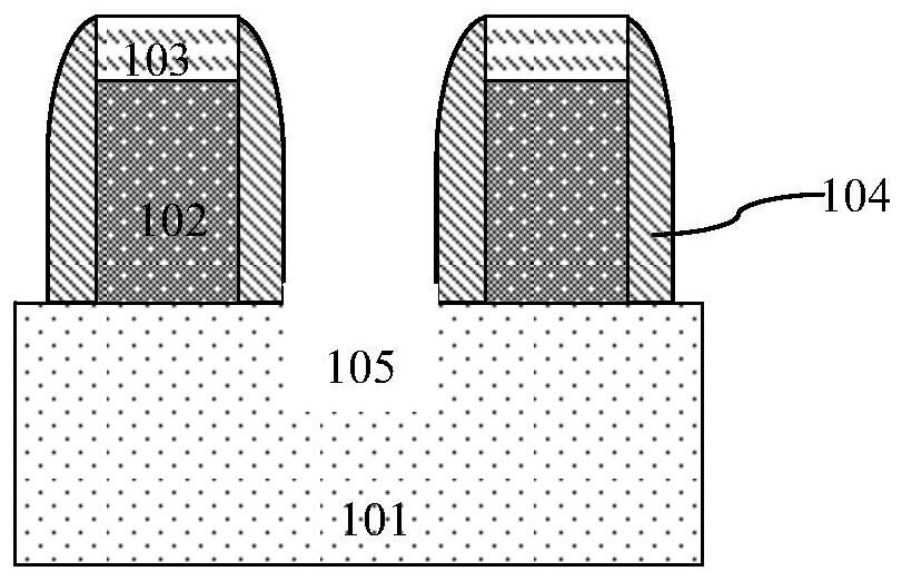
Figure 1 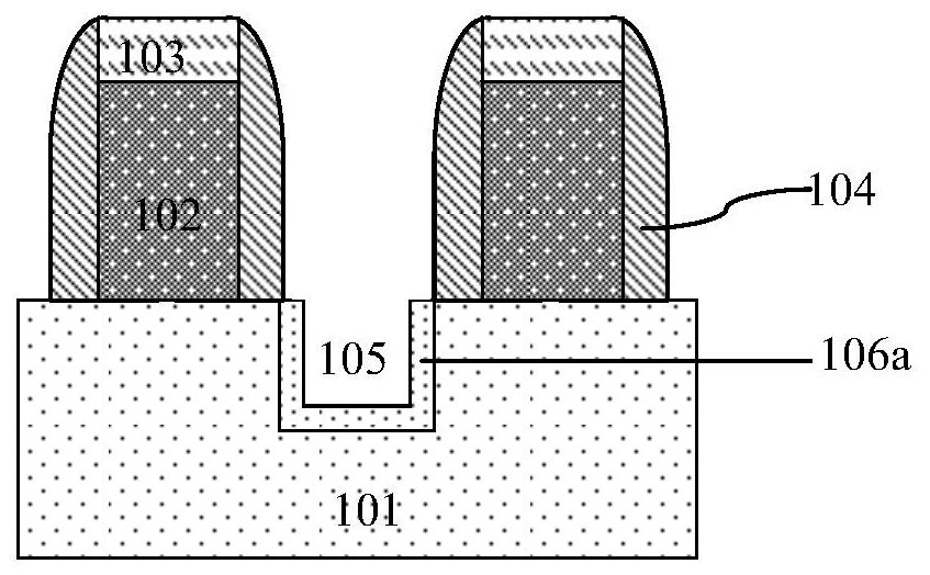
Figure 2 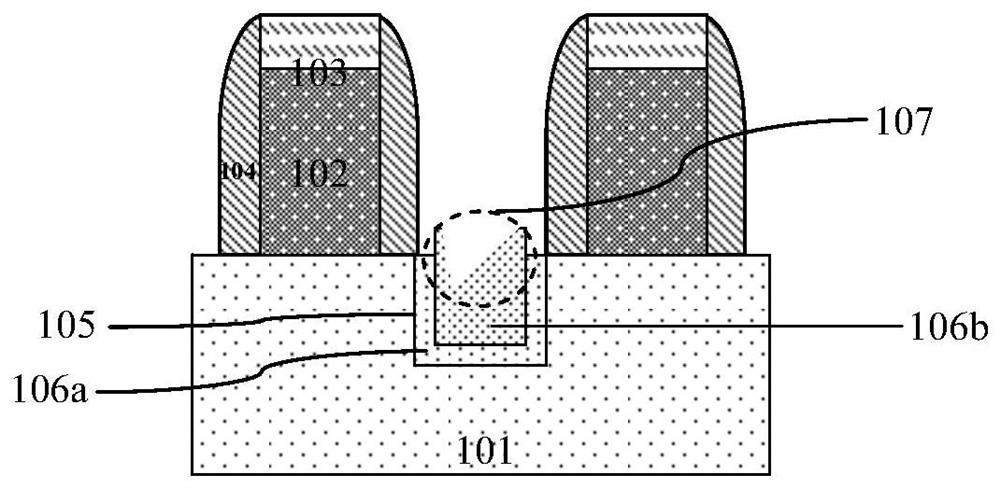
Figure 3
Abstract
Description
technical field
[0001] The invention relates to a method for manufacturing a semiconductor integrated circuit, in particular to a method for manufacturing an embedded epitaxial layer. Background technique
[0002] With the development of technology, the critical dimension (CD) of the device is getting smaller and smaller. When the process node of the device is below 28nm, it is often necessary to use embedded epitaxial layers in the source and drain regions to change the stress of the channel region, thereby increasing the current carrying capacity. Mobility of electrons and thus improve the performance of the device. For PMOS devices, the embedded epitaxial layer usually adopts silicon germanium epitaxial layer (SiGe); for NMOS devices, the embedded epitaxial layer usually adopts phosphorus silicon epitaxial layer (SiP).
[0003] Usually, after the gate structure of the device is formed, grooves are formed by self-alignment on both sides of the gate structure; then, an emb...
Examples
Embodiment Construction
[0064] Such as Figure 4 As shown, it is a flow chart of the manufacturing method of the embedded epitaxial layer 6 according to the embodiment of the present invention; as Figure 5A to Figure 5D As shown, it is a schematic diagram of the device structure in each step of the manufacturing method of the embedded epitaxial layer 6 in the embodiment of the present invention; the manufacturing method of the embedded epitaxial layer 6 in the embodiment of the present invention includes the following steps:
[0065] Step 1, such as Figure 5A As shown, the silicon substrate 1 is etched to form grooves 5 .
[0066] A gate structure is formed on the silicon substrate 1, and the groove 5 is self-aligned and formed on two sides of the gate structure.
[0067] The gate structure includes a gate dielectric layer and a polysilicon gate 2 stacked in sequence.
[0068] The top of the polysilicon gate 2 is covered with a top hard mask layer 3 , and side walls 4 are formed on the side of t...