
SiC MOSFET sub-module unit and crimping type package thereof
A crimp-type, sub-mold technology, applied in electrical components, semiconductor/solid-state device parts, semiconductor devices, etc., can solve the problem that silicon carbide devices are difficult to be crimped and packaged.
Patent Information
- Authority / Receiving Office
- CN · China
- Current Assignee / Owner
- Publication Date
- 2021-09-10
Smart Images
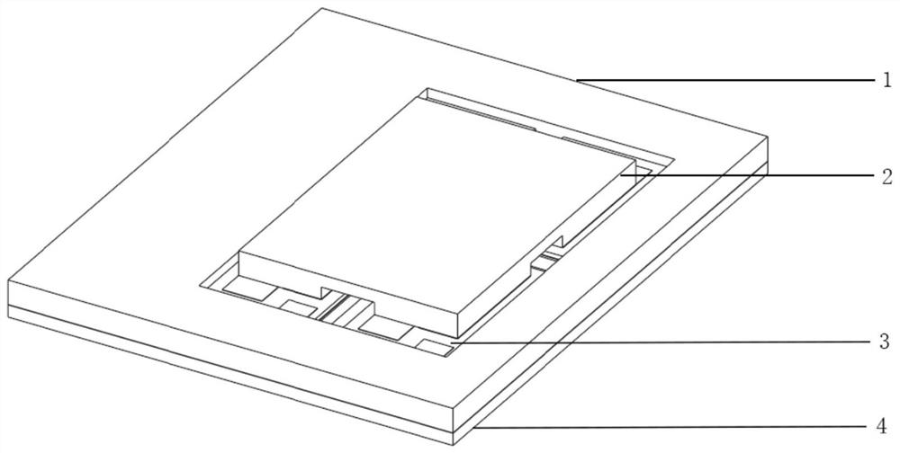
Figure 1 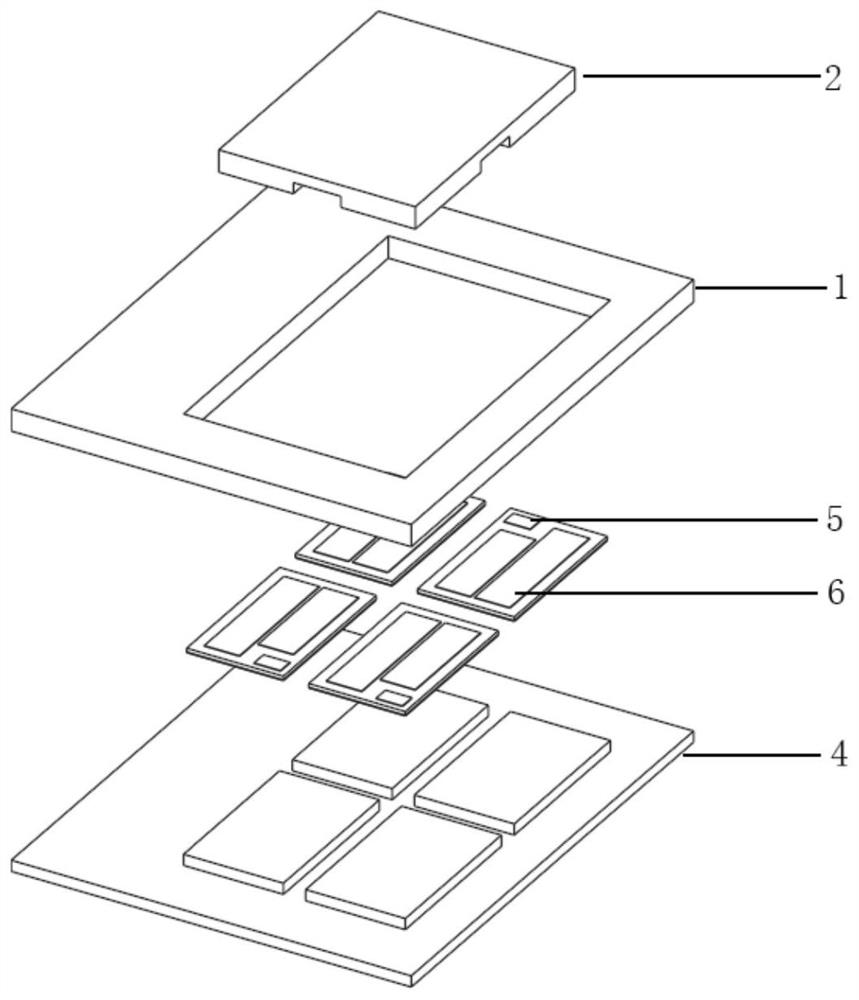
Figure 2 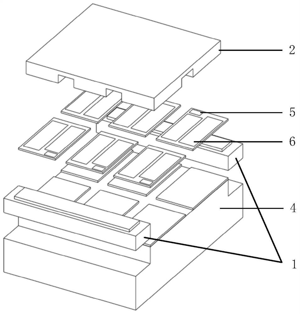
Figure 3
Abstract
Description
technical field
[0001] The invention belongs to the technical field of power semiconductor packaging, and in particular relates to a SiC MOSFET sub-module unit and a crimping type packaging thereof. Background technique
[0002] As a wide bandgap power semiconductor device, SiC MOSFET has many advantages over traditional silicon devices, such as higher operating temperature, lower on-state loss, higher switching frequency and greater critical breakdown field strength. With the gradual promotion of the application of silicon carbide power devices, there is no mature and unified form for the packaging of high-voltage silicon carbide power devices.
[0003] At present, the existing packaging forms of power devices are mainly divided into two types: soldering type packaging and crimping type packaging. Among them, the soldered package uses bonding wires to connect the chip to the power circuit. It is mainly used in medium and low voltage (650 to 3300V) application scenarios. In...
Examples
Embodiment Construction
[0040] Embodiments of the present invention are described in further detail below:
[0041] The SiCMOSFET sub-module unit designed in the present invention includes a source molybdenum sheet 2 , a SiCMOSFET chip array 3 , a DBC ceramic substrate 1 and a drain molybdenum sheet 4 . The lower surface of the source molybdenum sheet 2 is cut into four raised areas, and each raised area is respectively connected to the source 6 of the SiCMOSFET chip array 3 through nano-silver sintering, and does not cover the gate and terminal ; The SiCMOSFET chip array 3, each sub-module contains four pieces, one side of the source 6 faces upwards, and the grid 5 faces the outside, and is connected to the DBC ceramic substrate 1 on its periphery through bonding wires; the drain Pole molybdenum sheet 4, one side of which is connected to the drain of the SiCMOSFET chip array 3 through nano-silver sintering; The edge is a smooth arc; the internal gap of the SiCMOSFET sub-module unit 9 is filled with...