
Semiconductor structure and forming method thereof
A technology of semiconductor and through-hole interconnection structure, which is applied in the direction of semiconductor devices, semiconductor/solid-state device manufacturing, semiconductor/solid-state device components, etc., to achieve the effect of improving dimensional uniformity, process variation and process deviation
Patent Information
- Authority / Receiving Office
- CN · China
- Patent Type
- Applications(China)
- Current Assignee / Owner
- Publication Date
- 2021-10-22
Smart Images
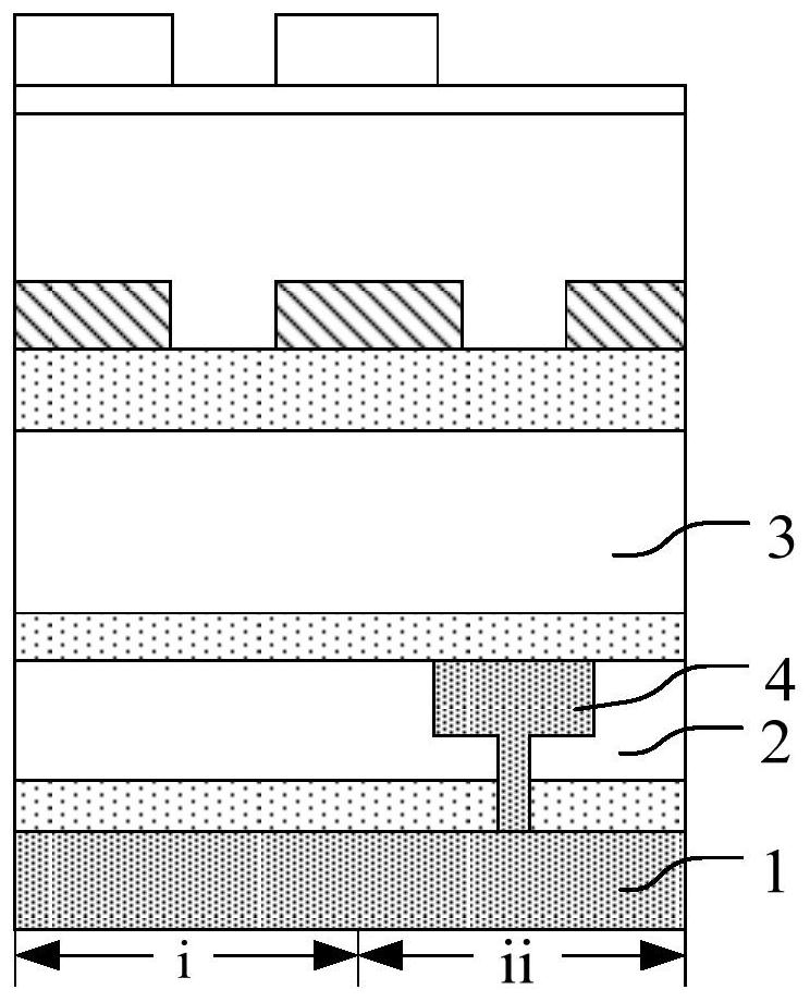
Figure 1 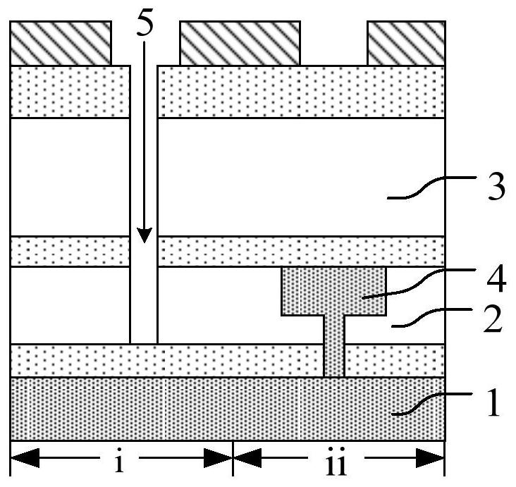
Figure 2 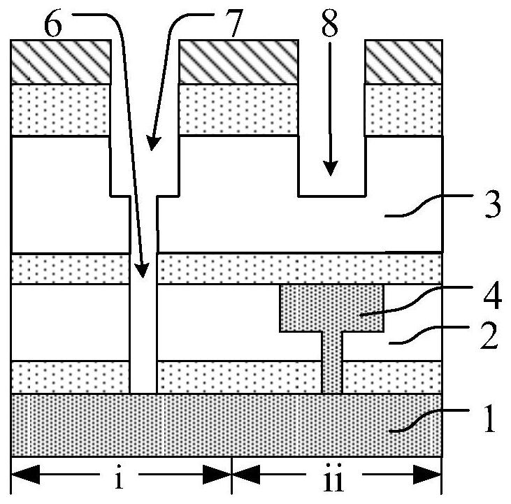
Figure 3
Abstract
Description
technical field
[0001] Embodiments of the present invention relate to the field of semiconductor manufacturing, and in particular, to a semiconductor structure and a method for forming the same. Background technique
[0002] Existing semiconductor structures generally consist of a semiconductor substrate and a plurality of dielectric layers and conductive layers formed on the semiconductor substrate. Specifically, multiple dielectric layers may be formed on the substrate by forming another dielectric layer on one dielectric layer, and each dielectric layer includes at least one metal line, and each of the at least one metal line includes A dielectric layer may be referred to as a metal layer. Existing semiconductor structures are generally composed of many metal layers, and metal lines in adjacent metal layers are usually electrically connected to each other through a via (Via) interconnection structure.
[0003] With the rapid growth of the semiconductor integrated circui...
Examples
Embodiment Construction
[0012] It can be seen from the background art that there are still great challenges in forming a super via interconnection structure. Specifically, the performance of the formed super via interconnection structure is poor, which in turn leads to poor interconnection performance of devices. The reason for the poor interconnection performance of the device is analyzed in combination with a method for forming a semiconductor structure.
[0013] refer to Figure 1 to Figure 5 , shows a structural schematic diagram corresponding to each step in a method for forming a semiconductor structure.
[0014] refer to figure 1 , providing a substrate (not shown), the substrate includes a first region i for forming a super via interconnection structure and a second region ii for forming a single-layer via interconnection structure; forming on the substrate The first interconnection 1, the dielectric stack 2 covering the first interconnection 1, and the second dielectric layer 3 covering t...