
Processing a workpiece with ozone and a halogenated additive
a technology of halogenated additives and workpieces, applied in the direction of sustainable manufacturing/processing, final product manufacturing, cleaning using liquids, etc., to achieve the effect of not easily removed, effective removal, and rapid and complete removal
Patent Information
- Authority / Receiving Office
- US · United States
- Patent Type
- Applications(United States)
- Current Assignee / Owner
- Publication Date
- 2005-02-17
- Estimated Expiration
- Not applicable · inactive patent
Smart Images
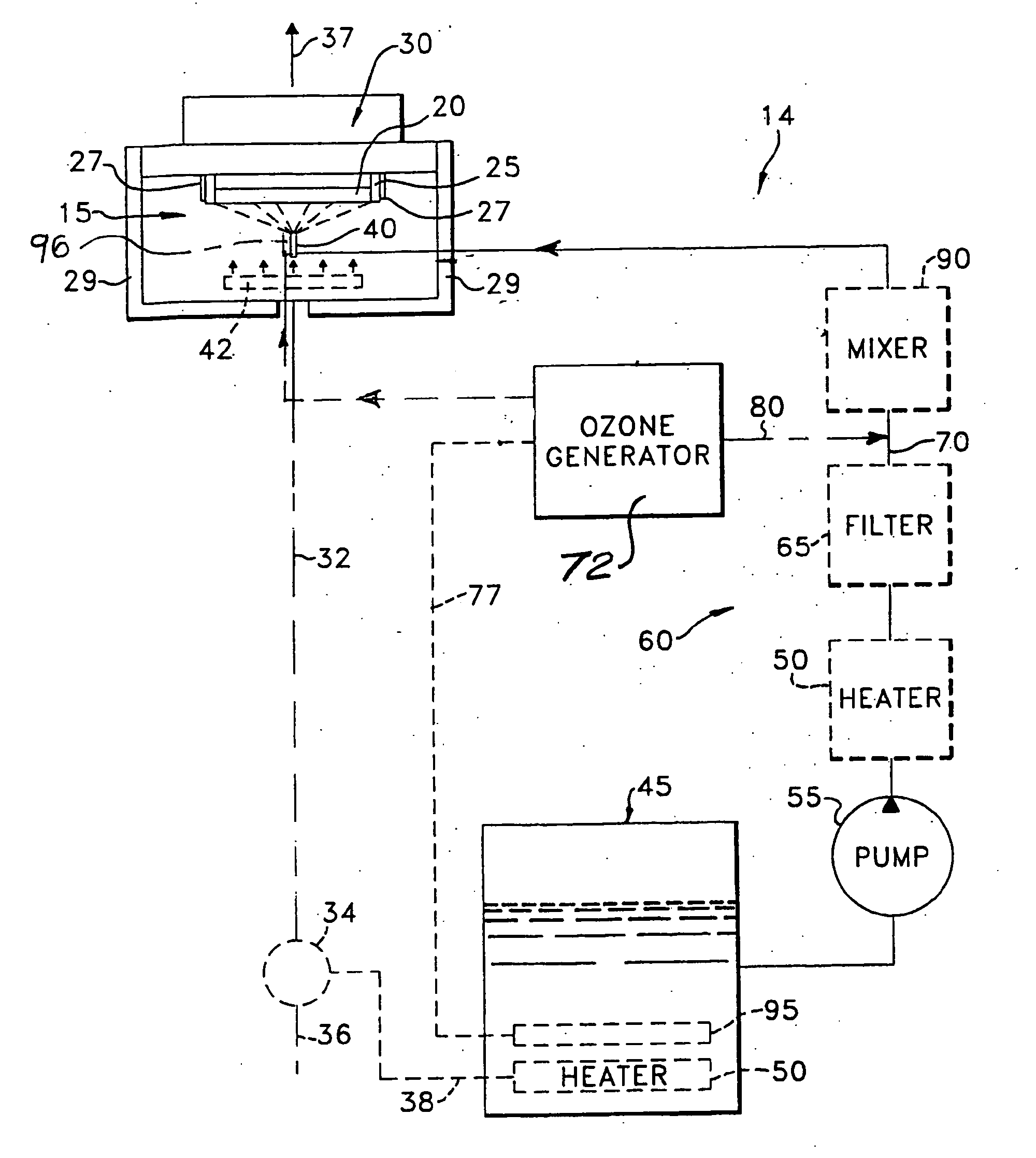
Figure 1 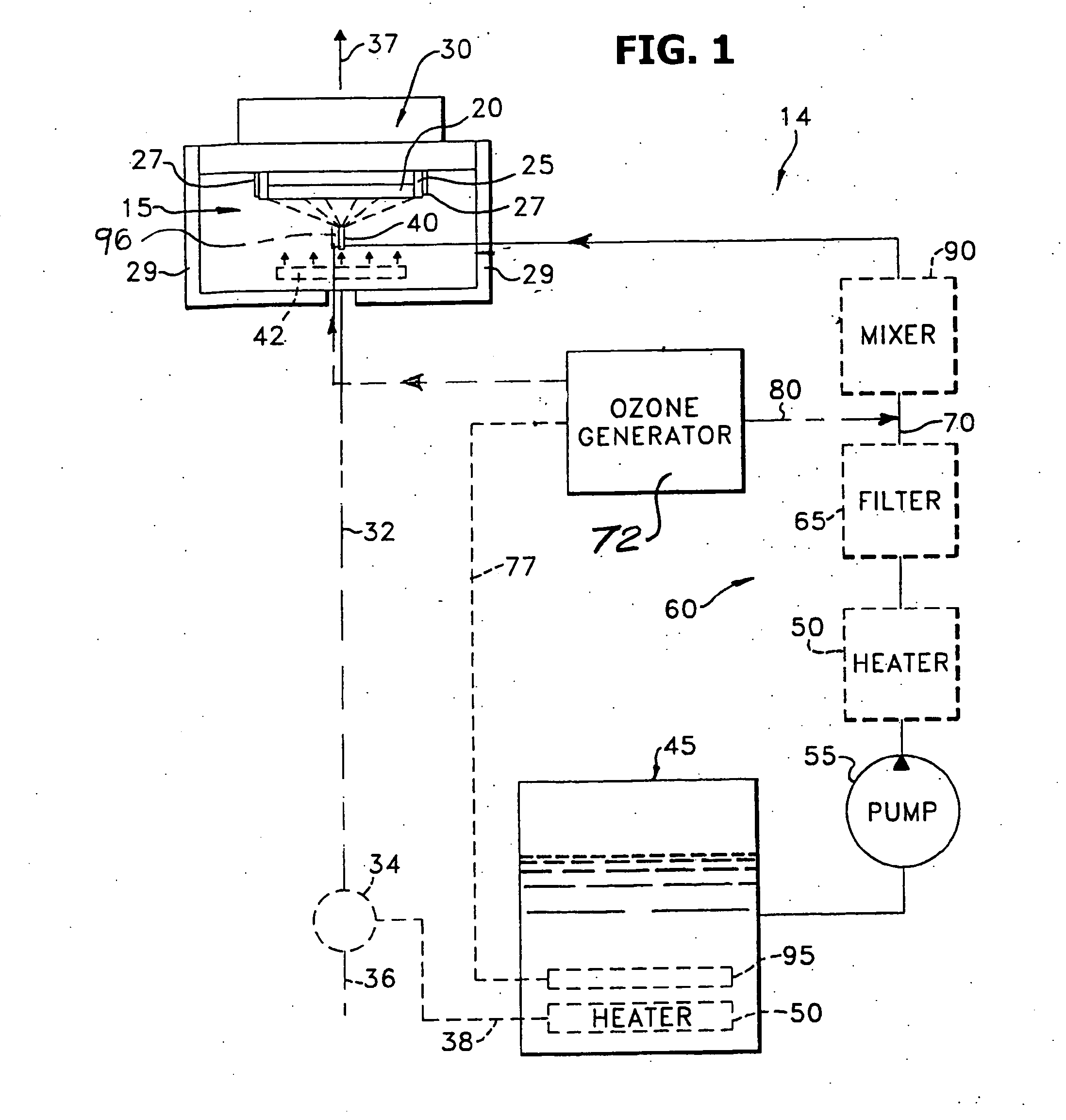
Figure 2 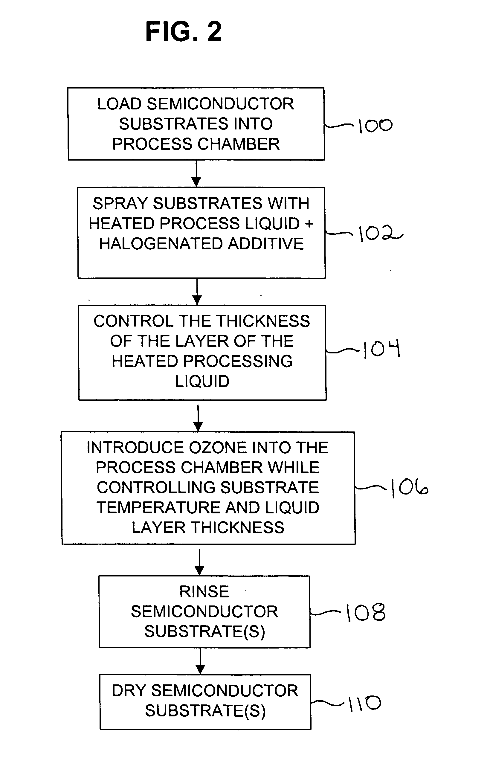
Figure 3
Abstract
Description
[0001] This Application is a Continuation of U.S. Patent Application Ser. No. 09 / 621,028, filed Jul. 21, 2000 and now pending, which is a Continuation-in-Part of International Patent Application PCT / US99 / 08516, filed Apr. 16, 1999, which is a Continuation-in-Part of U.S. patent application Ser. No. 09 / 061,318, filed Apr. 16, 1998, and now abandoned, which is a Continuation-in-Part of U.S. patent application Ser. No. 08 / 853,649, filed May 7, 1997, and now U.S. Pat. No. 6,240,933. Priority to each of these Applications is claimed under 35 U.S.C. §§ 119 and 120. These applications are also incorporated herein by reference.
[0002] Semiconductor devices are widely used in almost all consumer and home electronic products, as well as in communications, medical, industrial, military, and office products and equipment. Semiconductor devices are manufactured from semiconductor wafers. The wafers are typically round, flat silicon disks. The cleaning of semiconductor wafers is often a critical s...
Examples
Embodiment Construction
[0045] A silicon wafer having a hardened residual layer of photoresist about 1200A-1500A thick and an underlying SLAM (Sacrificial Light Absorbing Layer) layer about 2500 thick was processed as described above. SLAM is one form of an ARC or anti-reflective coating. The wafer was rotated at 1000 rpm. A solution of 49% (weight) HF in de-ionized water was further diluted to a concentration within the range of 0.01 to about 1% (by weight). This solution was heated to 90° C. and sprayed onto the spinning wafer at a flow rate of 500-800 ml / minute. Ozone gas was delivered into the process chamber at about 10 slpm and a concentration of 240 g / m3. The process was performed for 8:00 minutes. The photoresist layer and the SLAM layer were both removed. There was no detectable attack of the carbon doped oxide (CDO) dielectric layer.
[0046] Other halogenated additives, especially fluorinated additives, may be used instead of HF, for example NH4F. The ozone can be supplied dissolved in the water, ...