
System and method for cleaning semicondutor fabrication equipment parts
a technology for fabrication equipment and parts, applied in the direction of cleaning using liquids, inorganic non-surface active detergent compositions, instruments, etc., can solve the problems of contaminated equipment used in the semiconductor processing process, unusable, missed transfers, etc., to reduce cleaning defects, enhance cleaning process, and increase accuracy
Patent Information
- Authority / Receiving Office
- US · United States
- Patent Type
- Applications(United States)
- Current Assignee / Owner
- Publication Date
- 2005-03-03
- Estimated Expiration
- Not applicable · inactive patent
Smart Images
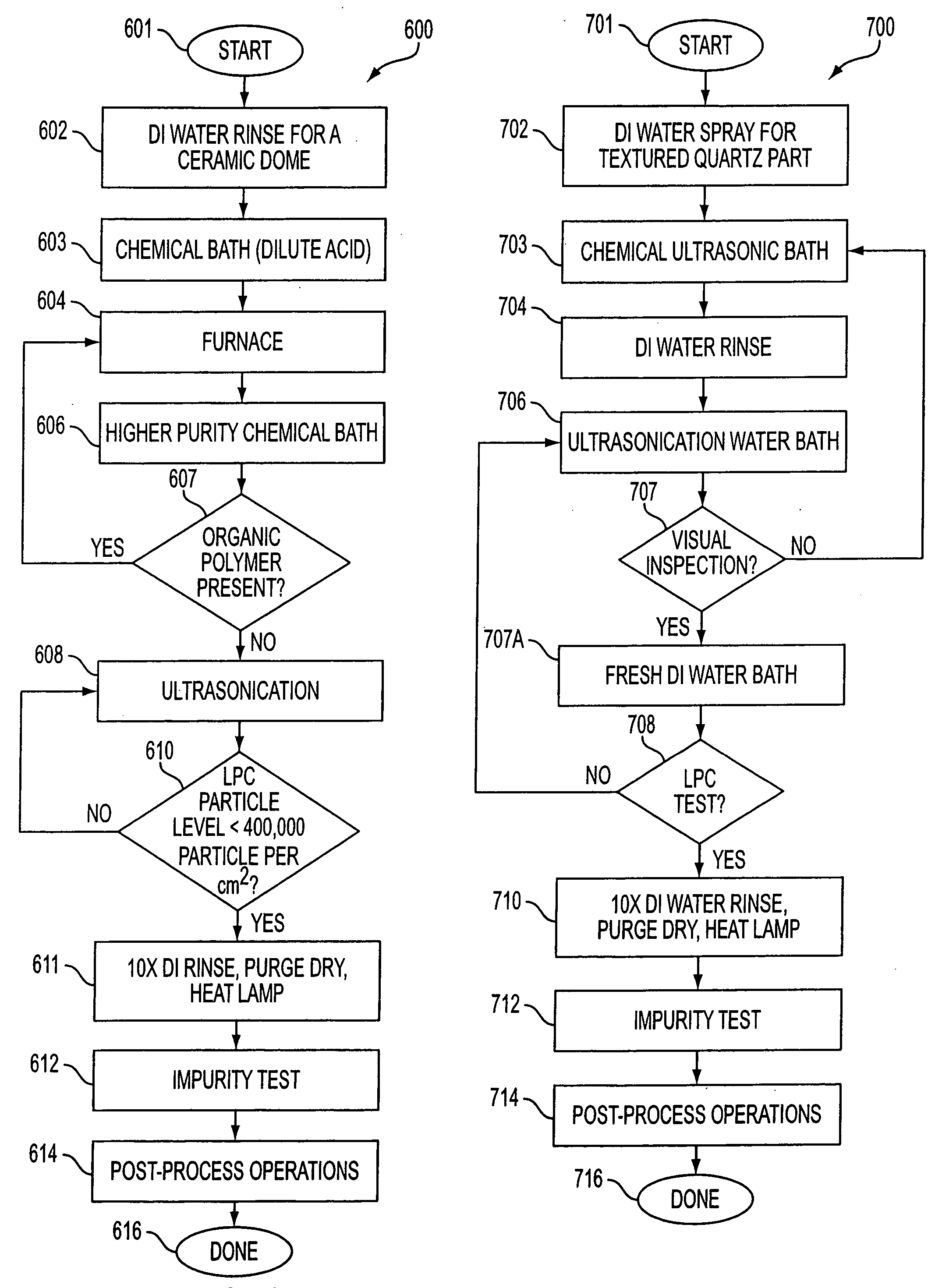
Figure 1 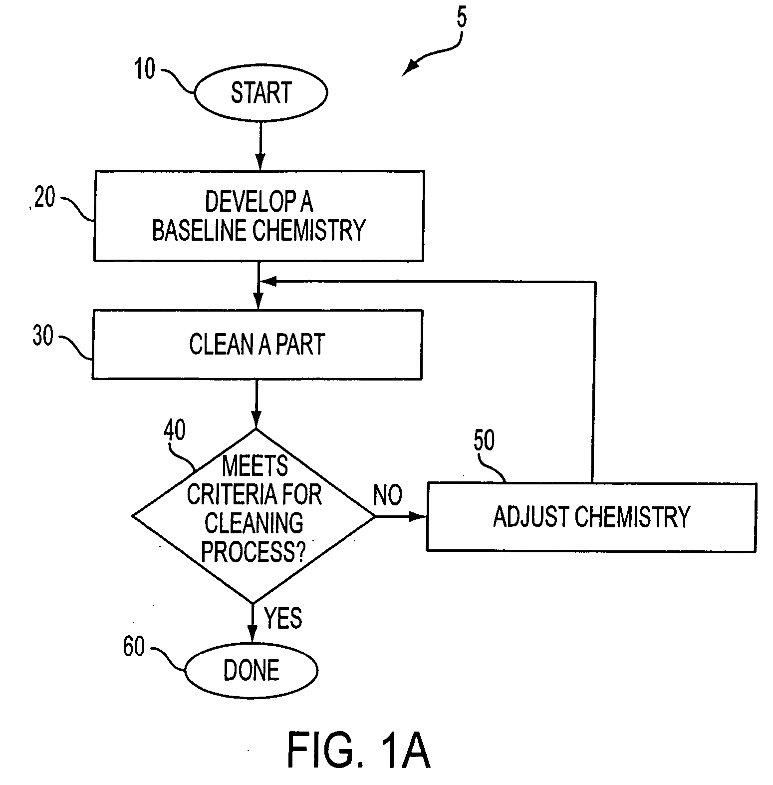
Figure 2 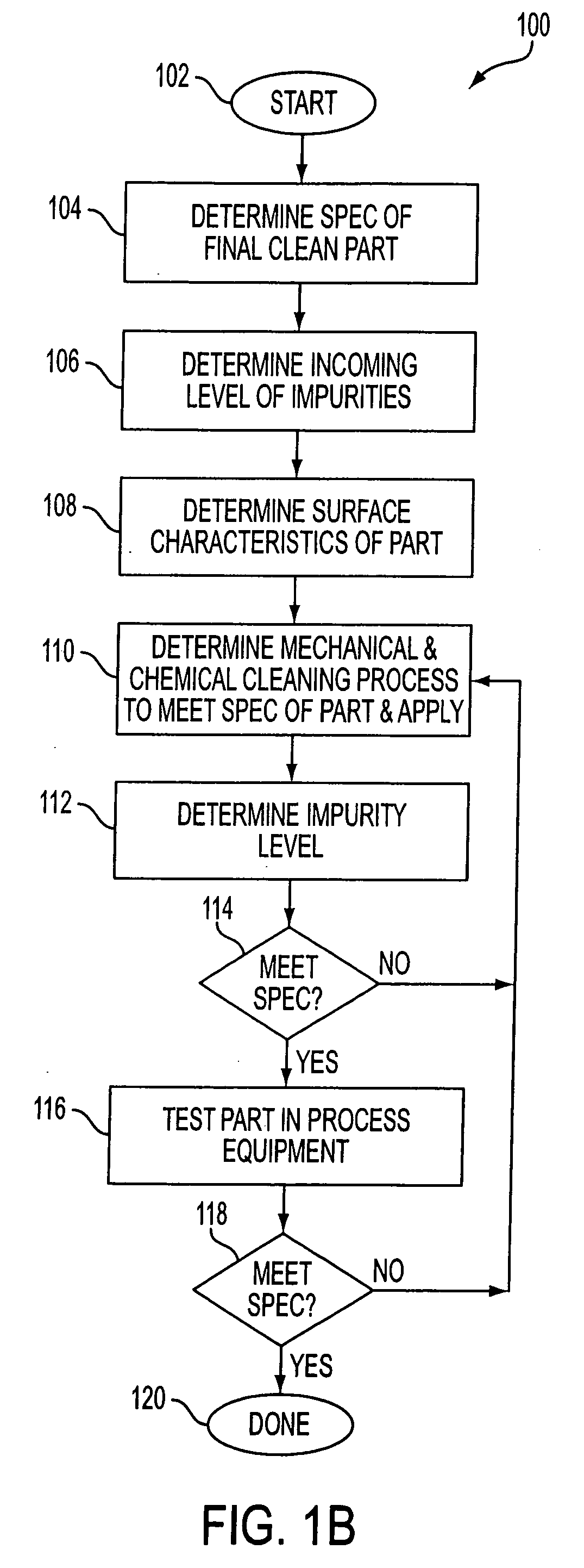
Figure 3
Abstract
Description
CROSS REFERENCE TO RELATED APPLICATIONS
[0001] This application claims the benefit of provisional application U.S. Ser. No. 60 / 224 / 582 (Atty. Docket No. 60081-300500), filed on Aug. 11, 2001, entitled “System and Method for Cleaning Semiconductor Fabrication Equipment Parts”, incorporated herein by reference.BACKGROUND OF THE INVENTION
[0002] The commercial fabrication of semiconductor chips is performed on silicon wafer substrates, which are typically four to twelve inches in diameter. There are often more than 100 processing steps in the fabrication of semiconductor chips including oxidation, diffusion, ion implantation, deposition of conductors and insulators, photolithography, and etching. Various conducting and insulating layers are deposited uniformly over the wafer to a thickness of a few microns.
[0003] In critical applications, certain new parts of semiconductor processing equipment need to be cleaned prior to installation and use in order to remove residual contamination f...
Examples
Embodiment Construction
[0024] An invention is described herein for cleaning semiconductor equipment parts (such as CVD and etch chamber parts) that achieve increased effectiveness in impurity removal. In the following description, numerous specific details are set forth in order to provide a thorough understanding of the present invention. It will be apparent, however, to those skilled in the art, that the present invention may be practiced without some or all of these specific details. In other instances, well known process steps have not been described in detail in order not to unnecessarily obscure the present invention. In particular, this includes most of the analytical testing methods used to measure or confirm impurity levels.
[0025] In accordance with one aspect of the present invention, the aforementioned metallic impurity removal is substantially enhanced by the use of a new chemical formula in the various cleaning processes. This cleaning formula is particularly novel as applied to the cleaning...