
Method for preventing contact defects in interlayer dielectric layer
a dielectric layer and interlayer technology, applied in the field of semiconductor/solid-state device manufacturing, can solve the problems of poor etching profile and etching defect in the substrate, serious obstacle in the alignment between each patterned layer, so as to improve the moisture absorption of the interlayer dielectric layer and increase the thermal stability of the dielectric layer
Patent Information
- Authority / Receiving Office
- US · United States
- Patent Type
- Applications(United States)
- Current Assignee / Owner
- Publication Date
- 2005-03-03
Smart Images
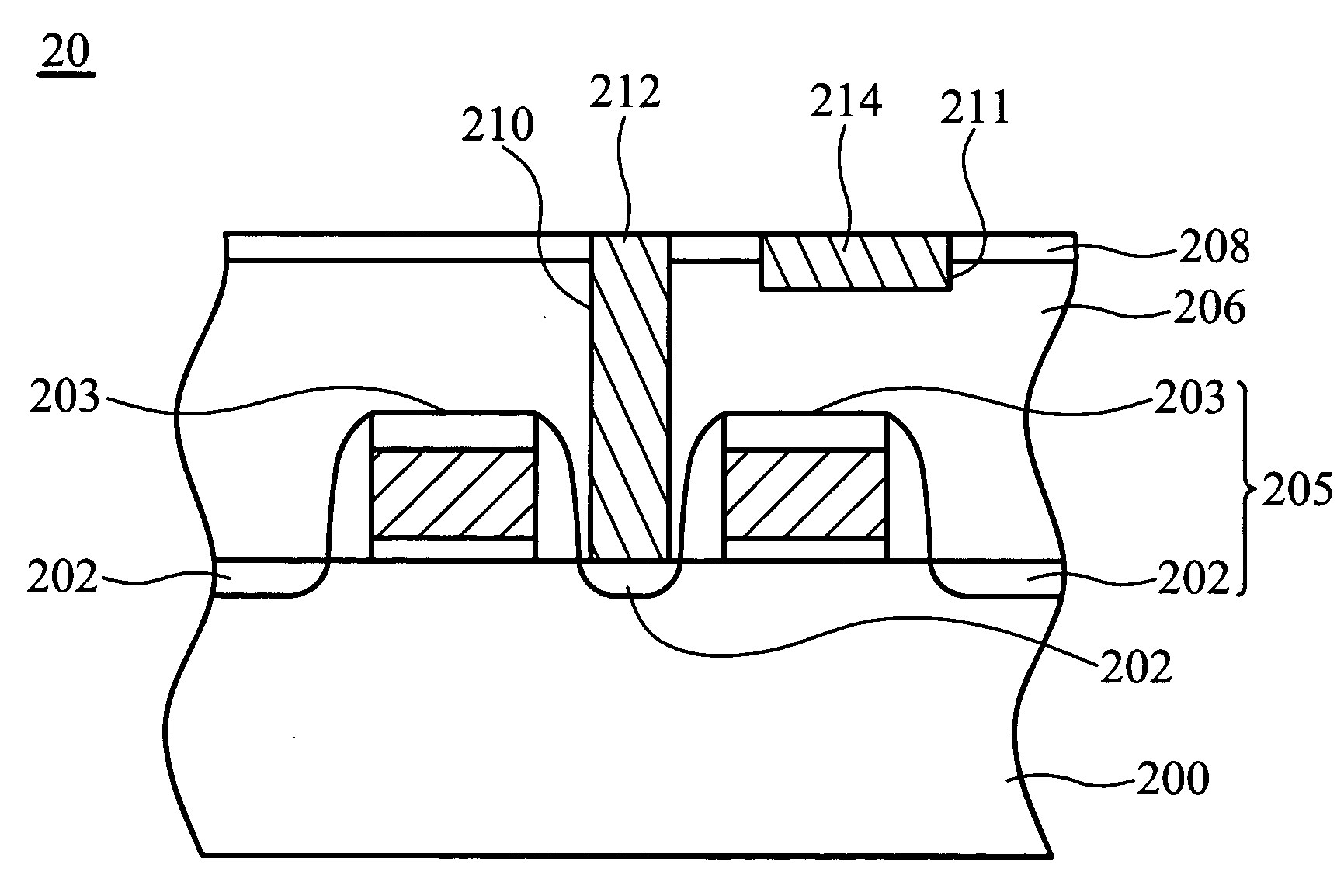
Figure 1 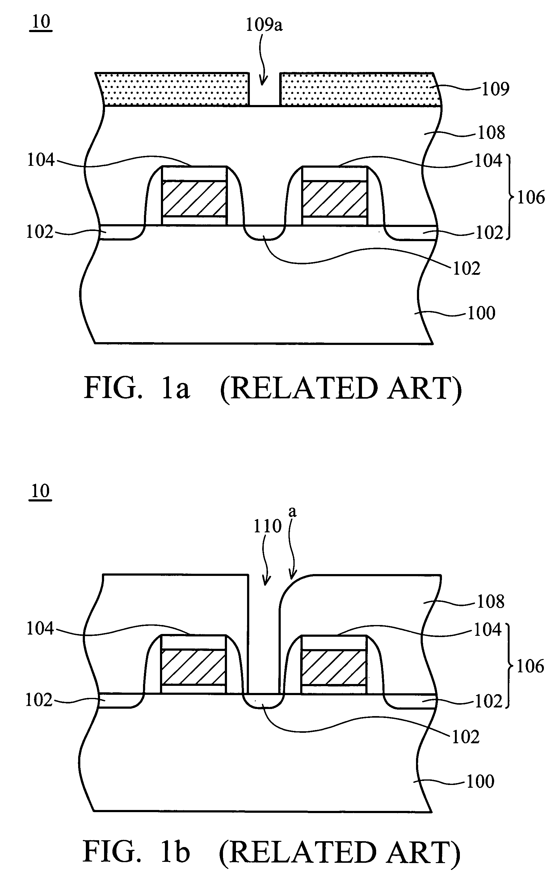
Figure 2 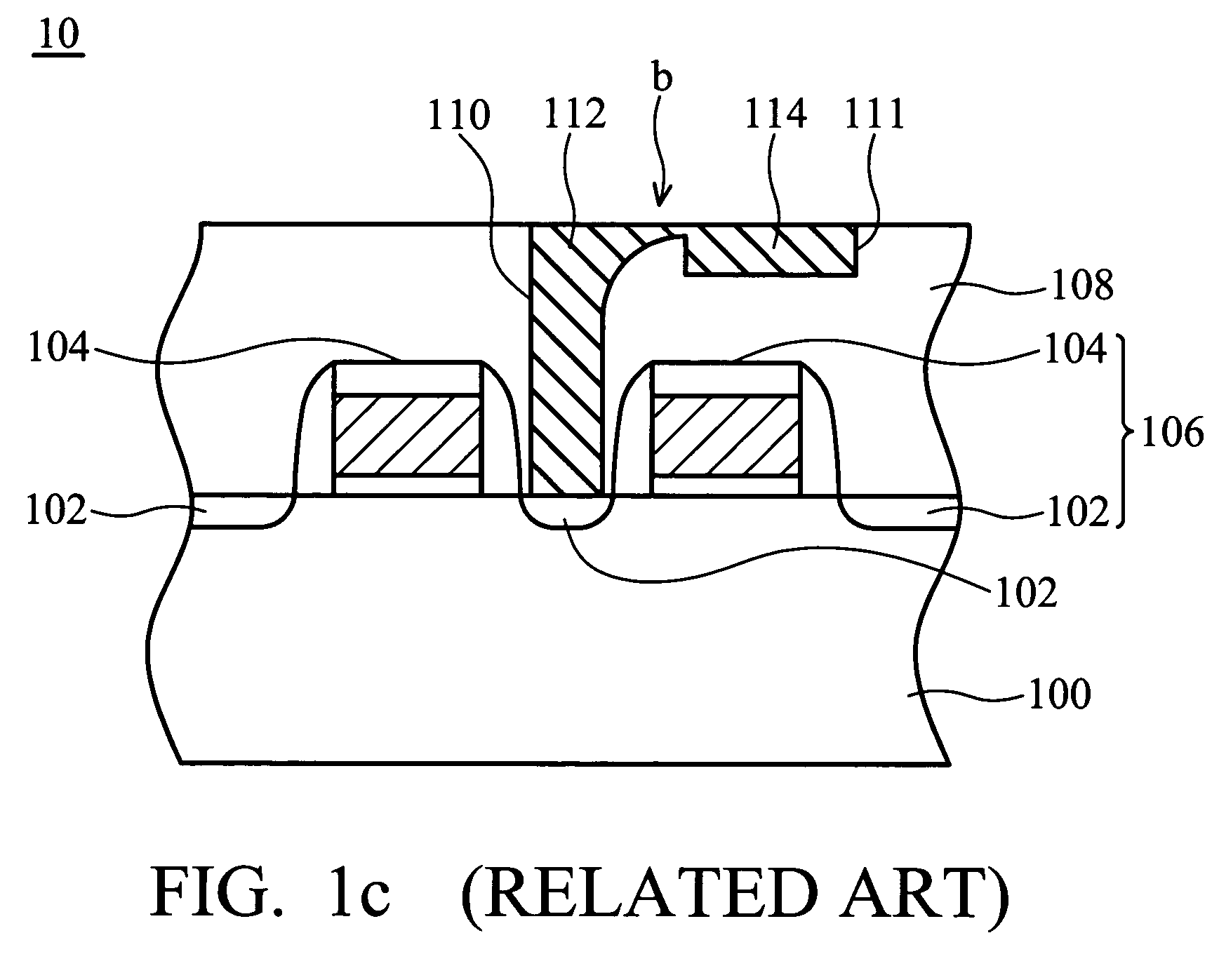
Figure 3
Abstract
Description
BACKGROUND OF THE INVENTION
[0001] 1. Field of the Invention
[0002] The present invention relates in general to a semiconductor process, and more particularly, to a method of forming an interlayer dielectric (ILD) layer and a method for preventing formation of etching defects in a contact.
[0003] 2. Description of the Related Art
[0004] As semiconductor device geometries continue to decrease in size to provide more devices per fabricated wafer and faster devices, misalignment between each patterned layer is a serious obstacle. Therefore, many self-aligned processes have been developed in order to prevent misalignment and decrease the interval between devices, thereby increasing the device density.
[0005] FIGS. 1a to 1c are cross-sections showing a conventional method of forming a substrate contact (Cs) for a memory device. First, in FIG. 1a, a silicon substrate 100, is provided. The substrate 100 may contain any semiconductor device, such as MOS transistors, and capacitors, used in t...
Examples
Embodiment Construction
[0021]FIGS. 2a to 2d are cross-sections showing a method of forming a substrate contact (Cs) for a memory device, such as a dynamic random access memory (DRAM), according to the invention.
[0022] First, in FIG. 2a, a substrate 200, such as a silicon substrate or other semiconductor substrate, is provided. The substrate 200 may contain any semiconductor devices, such as MOS transistors, and capacitors, used in the memory devices. Here, in order to simplify the diagram, only a flat substrate is depicted. Moreover, the substrate 200 has a peripheral circuit region 20.
[0023] Next, a plurality of transistors 205 composed of gate structures 203 and source / drain doping regions 202 is formed on the peripheral circuit region 20. The gate structure 203 is composed of a gate dielectric layer, a gate, a gate capping layer, and a gate spacer. The gate dielectric layer may be a silicon oxide layer formed by thermal oxidation. The gate may be a single polysilicon layer or a composite layer compos...