
Transistor
a transistor and gate electrode technology, applied in the field of transistors, can solve the problems of difficult downsizing of the contact hole and the distance between the contact hole and the gate electrode, and the difficulty of reducing the contact diameter and the precision, so as to reduce the layout area and reduce the area
Patent Information
- Authority / Receiving Office
- US · United States
- Patent Type
- Applications(United States)
- Current Assignee / Owner
- Publication Date
- 2005-05-05
Smart Images
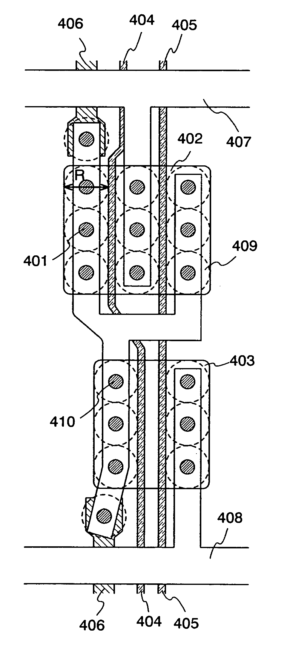
Figure 1 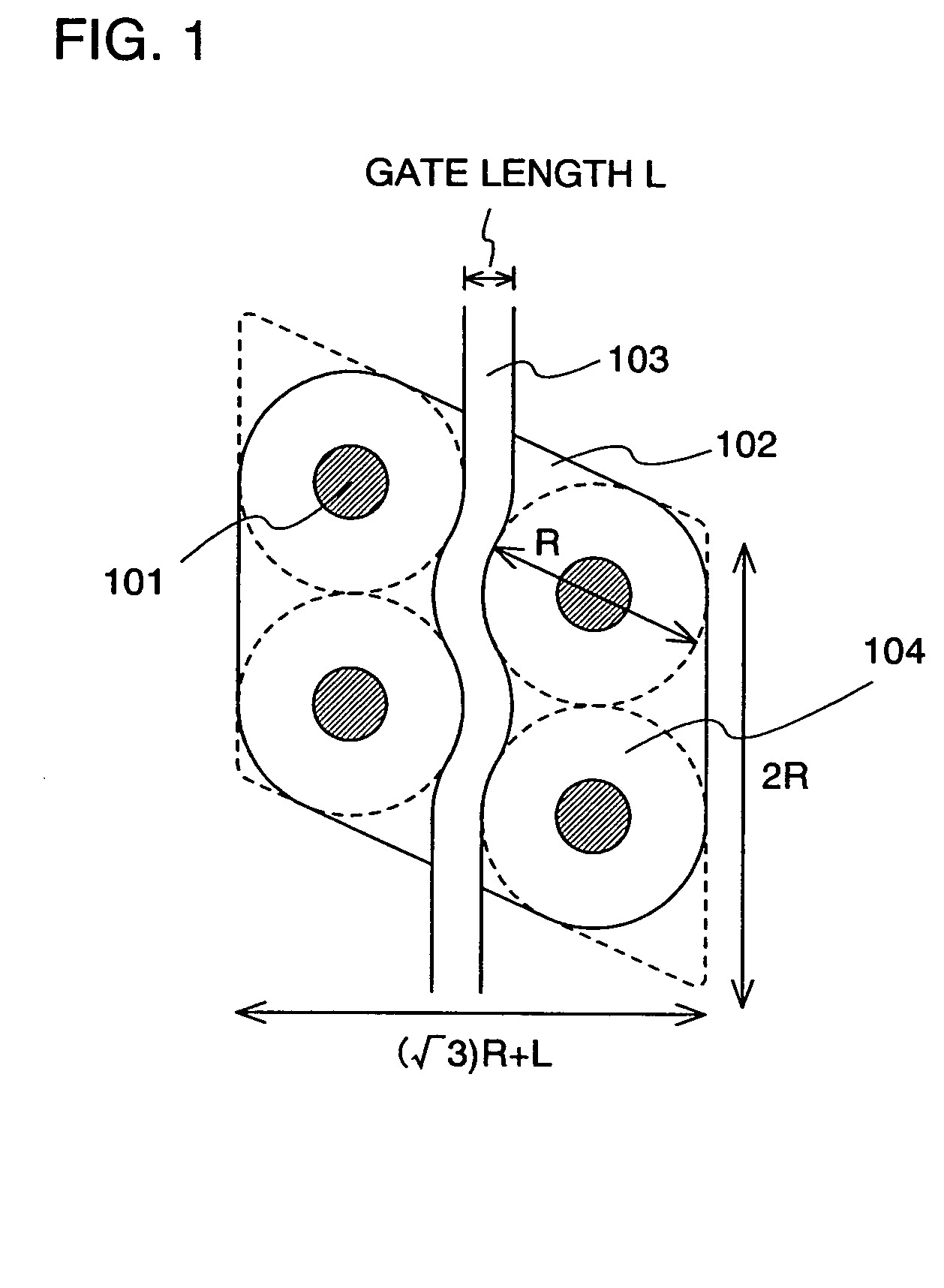
Figure 2 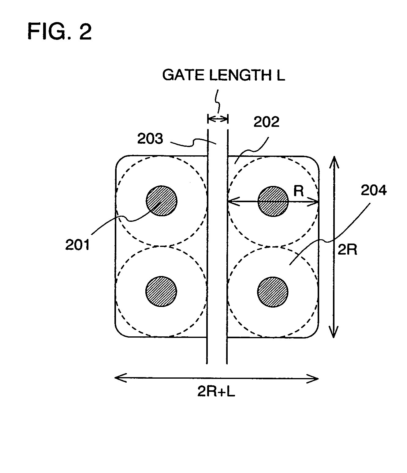
Figure 3
Abstract
Description
BACKGROUND OF THE INVENTION
[0001] 1. Field of the Invention
[0002] The present invention relates to a transistor whose area is to be reduced.
[0003] 2. Description of the Related Art
[0004] In recent years, downsizing of a gate electrode has been advanced by a technique of slimming, in which a line width is narrowed after the pattern formation using an exposure unit, and the like. Meanwhile, a contact diameter and a distance between a contact hole and a gate electrode are difficult to be reduced to the precision higher than the exposure precision, and in an LSI (Large Scale Integration) on a single-crystalline silicon substrate, downsizing is achieved by a technique of a self-alignment contact and the like. However, when a self-alignment contact technology cannot be employed because of a reason of a process, a design rule that a contact diameter is much larger than a gate length is required to be adopted. The design rule in such a case is, for example, that a contact diameter is ap...
Examples
embodiment 1
[Embodiment 1]
[0035] The invention is also effective for a transistor with a double-gate structure.
[0036] In a transistor shown in FIG. 7 that is a conventional transistor with a double-gate structure, six contacts 301 and two gate electrodes 303 are arranged on an active region 302. A region 304 including a margin for a contact is assumed to be a circle having a diameter of R, which is denoted by a dotted line. In the transistor shown in FIG. 7, the regions 304 each including a margin for a contact are arranged to be a tetragonal lattice when a gate length L and a distance d between the gate electrodes are not considered. In that case, the area of the active region 302 is approximately 3R×(2R+2L+d).
[0037] In a transistor shown in FIG. 3 that is a transistor with a double-gate structure according to the invention, six contacts 311 and two gate electrodes 313 are arranged on an active region 312. A region 314 including a margin for a contact is assumed to be a circle having a diame...
embodiment 2
[Embodiment 2]
[0040] Described below is an example in which the area of a logic gate is practically reduced by applying a transistor according to the invention.
[0041]FIG. 4A shows an example of a layout of a conventional two-input NAND gate, comprising two P-channel TFTs and two N-channel TFTs. The two P-channel TFTs include an active region 402, a contact 401, and a gate electrode connected to input signal lines 404 and 405, while the two N-channel TFTs include an active region 403, a contact 410, and a gate electrode connected to the input signal lines 404 and 405.
[0042] In each of the two P-channel TFTs, one of a pair of impurity regions is connected to a power supply line 407. The two N-channel TFTs are connected in series to each other and one of impurity regions at both ends is connected to a ground line 408. The other impurity region of each P-channel TFT and the other of the impurity regions of the N-channel TFTs connected in series are connected to an output signal line 4...
embodiment 3
[Embodiment 3]
[0056] Electronic devices employing a transistor according to the invention include a video camera, a digital camera, a goggle type display (head mounted display), a navigation system, a sound reproducing device (a car audio equipment, an audio set, and the like), a computer, a game machine, a portable information equipment (a mobile computer, a mobile phone, a portable game machine, an electronic book, and the like), an image reproducing device including a recording medium (more specifically, a device which can reproduce a recording medium such as a digital versatile disc (DVD), and which includes a display for displaying the reproduced image), or the like. Specific examples of the electronic apparatuses are illustrated in FIGS. 8A to 8E.
[0057]FIG. 8A illustrates a portable information terminal which includes a main body 2001, a display portion 2002, an operating key 2003, a modem 2004, and the like. Although the modem 2004 is removable in the portable information te...