
Silicon wafer, its manufacturing method, and its manufacturing apparatus
Patent Information
- Authority / Receiving Office
- US · United States
- Current Assignee / Owner
- Publication Date
- 2006-01-26
- Estimated Expiration
- Not applicable · inactive patent
Smart Images
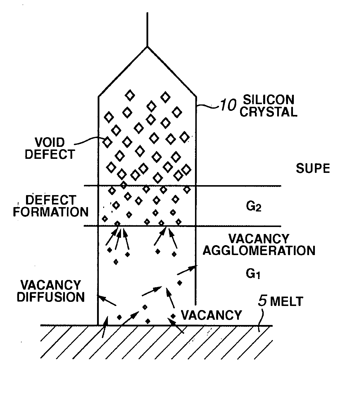
Figure 1 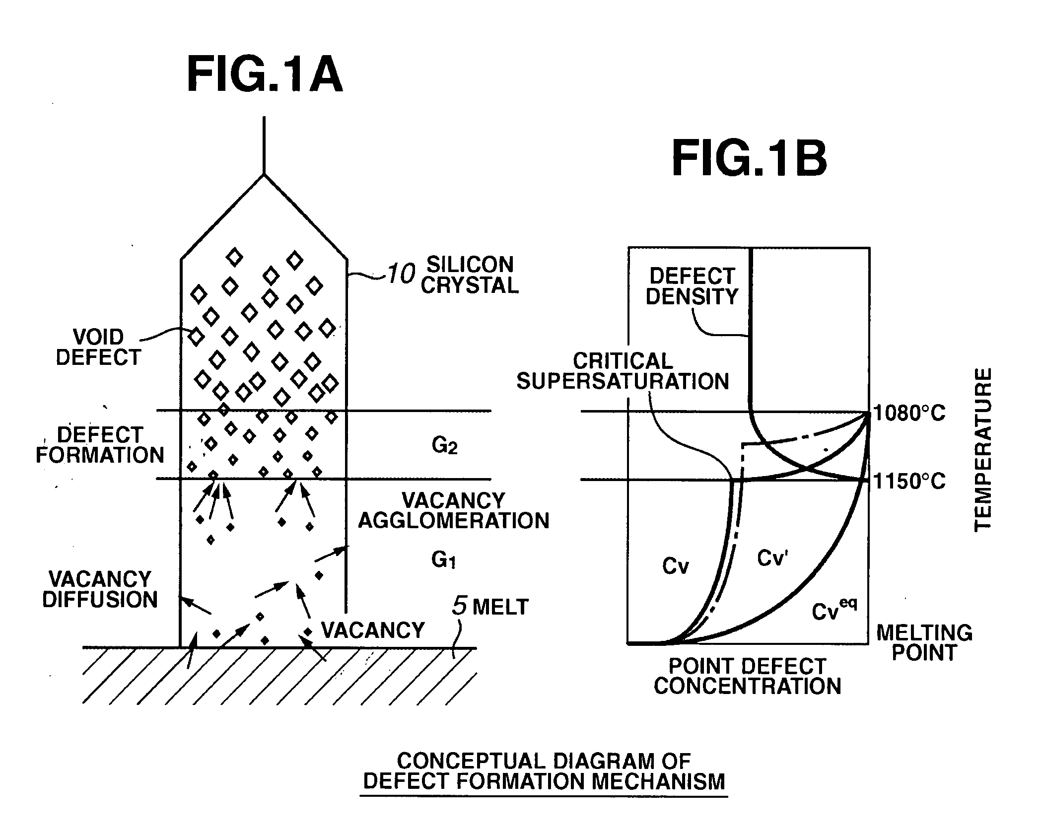
Figure 2 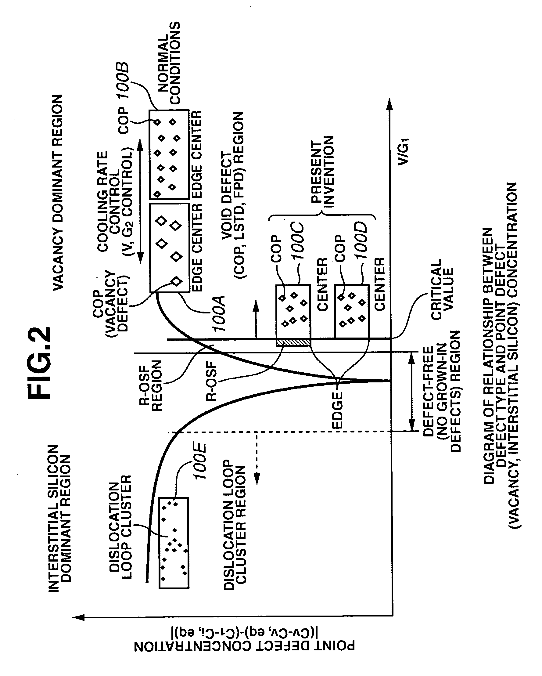
Figure 3
Abstract
Description
TECHNICAL FIELD
[0001] This invention relates to a silicon wafer, its manufacturing method and its manufacturing apparatus, and more particularly relates to a manufacturing method and a manufacturing apparatus with which the size and density of void defects can be reduced, and to a silicon wafer manufactured with these method and apparatus. The present invention also relates to a method for manufacturing a silicon single crystal, and to a silicon single crystal, and more particularly relates to a method for manufacturing a defect-free silicon single crystal in which void defects, OSFs (oxidation induced stacking faults), and dislocation clusters (interstitial silicon dislocation defects) have been eliminated, and to a defect-free silicon single crystal manufactured by this method, and to an apparatus for pulling this defect-free silicon single crystal. BACKGROUND ART
[0002] Silicon crystals are manufactured by pulling according to the CZ (Czochralski) method. An ingot of a pulled si...
Examples
first embodiment
[0185]100D shown in FIG. 2 is a silicon wafer in the first embodiment. The silicon wafer 100D in this embodiment is manufactured such that no OSF region is present anywhere in the plane of the silicon wafer, from the planar center to the edge.
[0186] The region indicated by hatching in FIG. 5 indicates the range of the average void defect density and the average void defect size in the entire plane of the silicon wafer 100D of the first embodiment. The silicon wafer 100D of the present invention has an average void defect density in the entire wafer plane of 5×10⁶ / cm3 or less, and has an average void defect size of 100 nm or less.
[0187] The silicon crystal 10 in the first embodiment has a diameter of 200 mm, and is grown by pulling at a rate V of from 1.11 to 1.45 mm / min.
[0188] With this first embodiment, since the average void defect density in the entire wafer plane is 5×10⁶ / cm3 or less, and the average void defect size is 100 nm or less, deterioration in device characteristics ...
second embodiment
[0267]100C in FIG. 2 is the silicon wafer in the second embodiment. The silicon wafer 100C in this embodiment is manufactured such that no OSFs are present in the plane of the wafer at least from the center of the plane up to 10 mm from the outer periphery.
[0268] The region indicated by hatching in FIG. 5 indicates the range of the average void defect density and the average void defect size in the region to the inside of R-OSF of the silicon wafer 100C of the second embodiment. The silicon wafer 100C in the second embodiment has an average void defect density in the region to the inside of R-OSF of 5×10⁶ / cm3 or less, and has an average void defect size of 100 nm or less.
[0269] The manufacturing method in the second embodiment is as follows.
Manufacturing Method 3
[0270] With this Manufacturing Method 3, the above-mentioned method ⑤ is applied, and the cooler 30 is installed inside the CZ furnace 2. The diameter of the silicon crystal 10 is 200 mm.
[0271] The pulling rate V of th...
third embodiment
[0282] We will now describe an embodiment in which it is possible to expand the allowable range of the growth condition V / G at which a defect-free crystal can be obtained.
[0283]FIG. 25 is a side view of the apparatus constitution in this embodiment.
[0284] As shown in FIG. 25, the single crystal pulling apparatus 101 of this embodiment is equipped with a CZ furnace 102 as a chamber for pulling a single crystal.
[0285] A crucible 103a, in which the raw material polycrystalline silicon is melted and held as a melt 105, is provided inside the CZ furnace 102. The outside of the quartz crucible 103a is covered by a graphite crucible 103b. A main heater 109 for heating and melting the polycrystalline silicon raw material in the quartz crucible 103a is provided to the side on the outside of the quartz crucible 103b.
[0286] An insulating cylinder 113 is provided between the main heater 109 and the inner walls of the CZ furnace 102. A pulling mechanism (not shown) is provided above the quar...