
Ceramic capacitor
Patent Information
- Authority / Receiving Office
- US · United States
- Current Assignee / Owner
- Publication Date
- 2007-03-22
Smart Images
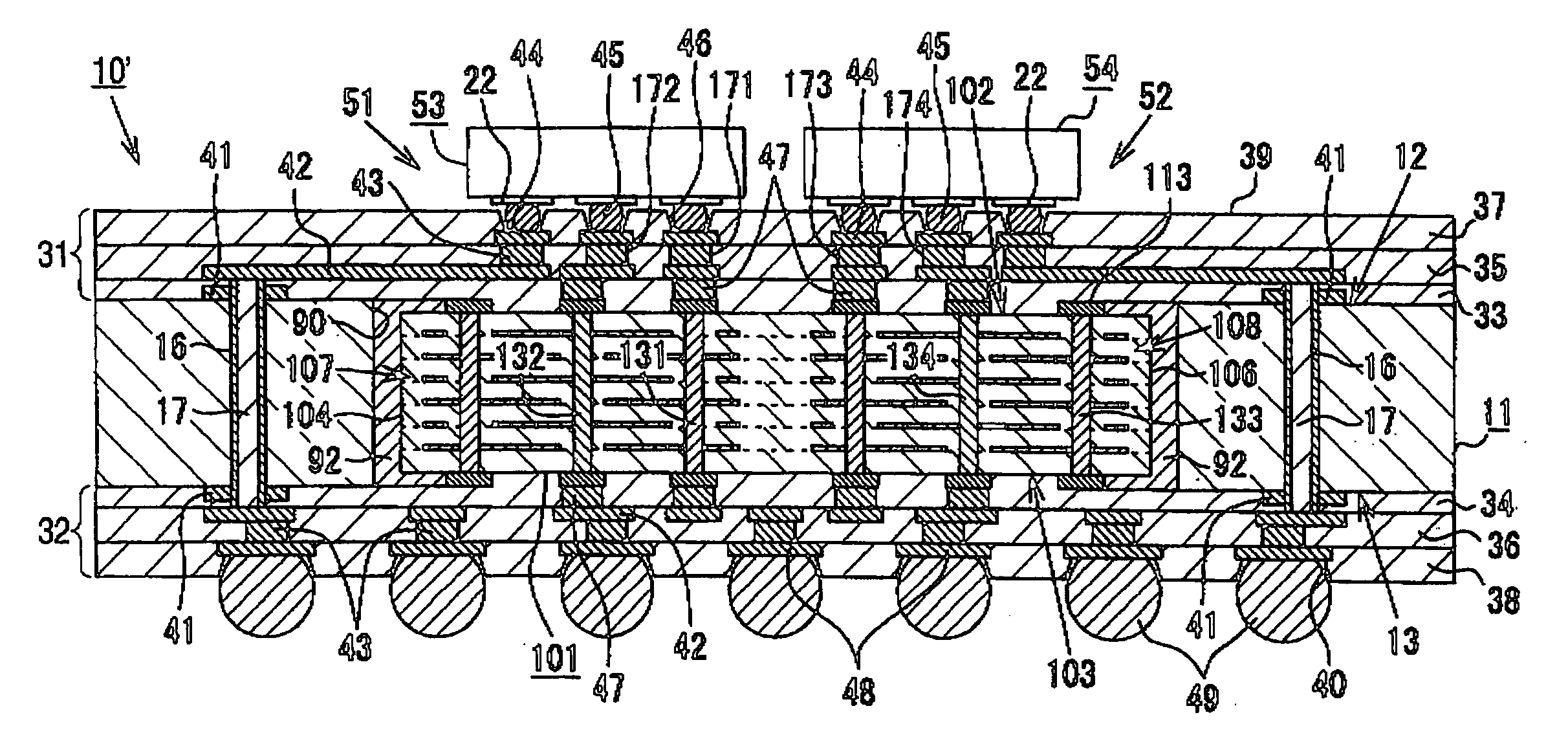
Figure 1 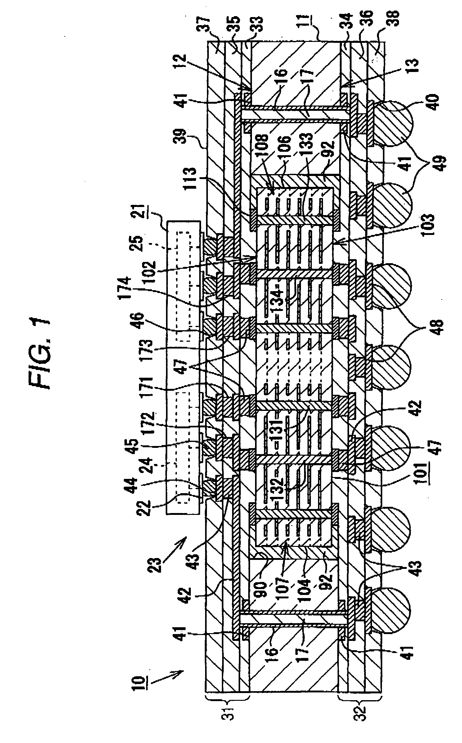
Figure 2 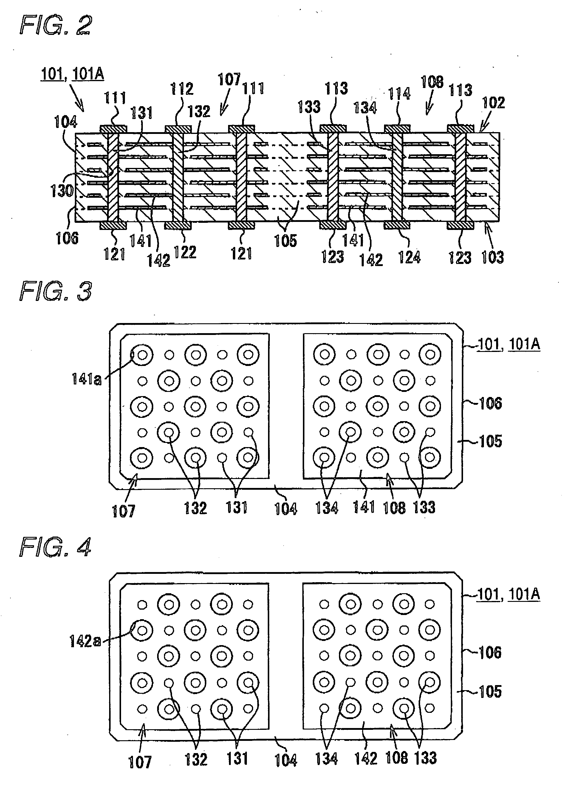
Figure 3
Abstract
Description
FIELD OF THE INVENTION
[0001] The present invention relates to a circuit board having a structure in which a ceramic capacitor is buried in a board core, a buildup layer is stacked on the surface thereof, and a semiconductor integrated circuit device is mounted thereon, and a ceramic capacitor used in the circuit board. BACKGROUND OF THE INVENTION
[0002] With recent enhancement in speed and performance of semiconductor integrated circuit devices (IC chips) used in micro processors of computers and the like, the number of terminals tends to increase and the pitch between terminals tends to decrease accordingly. In general, a plurality of terminals is densely arranged in an array on the bottom surface of an IC chip and the terminal group is connected to the terminal group of a mother board in a flip chip manner. However, since the terminal group of the IC chip and the terminal group of the mother board are greatly different from each other in pitches between the terminals, a method of...
Examples
first embodiment
[First Embodiment]
[0108] Hereinafter, a circuit board according to a first embodiment of the present invention will be described in detail with reference to the attached drawings.
[0109] As shown in FIG. 1, a circuit board 10 according to the first embodiment is a circuit board for mounting an JC chip and includes a substantially rectangular panel-shaped board core 11 made of glass epoxy, a first buildup layer 31 (buildup layer) formed on the top surface 12 (main core surface) of the board core 11, and a second buildup layer 32 formed on the bottom surface 13 (rear core surface) of the board core 11. Through-hole conductors 16 are formed at a plurality of positions in the board core 11. The through-hole conductors 16 electrically connect the top surface 12 of the board core 11 to the bottom surface 13. The insides of the through-hole conductors 16 are filled with a filler 17 such as epoxy resin. Patterned conductor layers 41 made of copper are formed on the top surface 12 and the bo...
second embodiment
[Second Embodiment]
[0147] Hereinafter, a circuit board according to a second embodiment of the invention will be described in detail with reference to the drawings.
[0148] As shown in FIG. 8, a circuit board 10′ according to the second embodiment has two IC chip mounting regions 51 and 52 (semiconductor integrated circuit device mounting regions) on the surface 39 of the first buildup layer 31. Instead of the IC chip 21 in the first embodiment, two IC chips 53 and 54 having only one processor core are mounted on the IC chip mounting regions 51 and 52, respectively.
[0149] A part of each first power-supply via conductor 131 constituting the capacitor function unit 107 is electrically connected to the corresponding surface connection terminal 22 of the IC chip 53 through the corresponding first power-supply electrode terminal 111 and the corresponding first power-supply conductor portion 171. A part of each first ground via conductor 132 constituting the capacitor function unit 107 is...
third embodiment
[Third Embodiment]
[0173] Hereinafter, a circuit board according to a third embodiment of the invention will be described in detail with reference to the drawings.
[0174]FIG. 23 illustrates a circuit board 10A according to the third embodiment, which is different from the circuit board 10 according to the first embodiment shown in FIG. 1 in that the IC chip 21 has two I / O circuit units 28 and 29, in addition to two processor cores 24 and 25. FIGS. 2 to 4 illustrating the ceramic capacitor 101 and the details thereof and FIGS. 5 to7 illustrating the manufacturing method and the details thereof are adapted to the ceramic capacitor 101A according to the third embodiment, which is different from the ceramic capacitor 101 according to the first embodiment in that the following facts.
[0175]FIG. 24 illustrates the ceramic capacitor 101A according to the third embodiment. In the ceramic capacitor 101A according to the embodiment, an extra-system capacitor function unit 162 (for supplying an...