
Optoelectronic device chip having a composite spacer structure and method making same
Patent Information
- Authority / Receiving Office
- US · United States
- Current Assignee / Owner
- Publication Date
- 2007-11-22
Smart Images
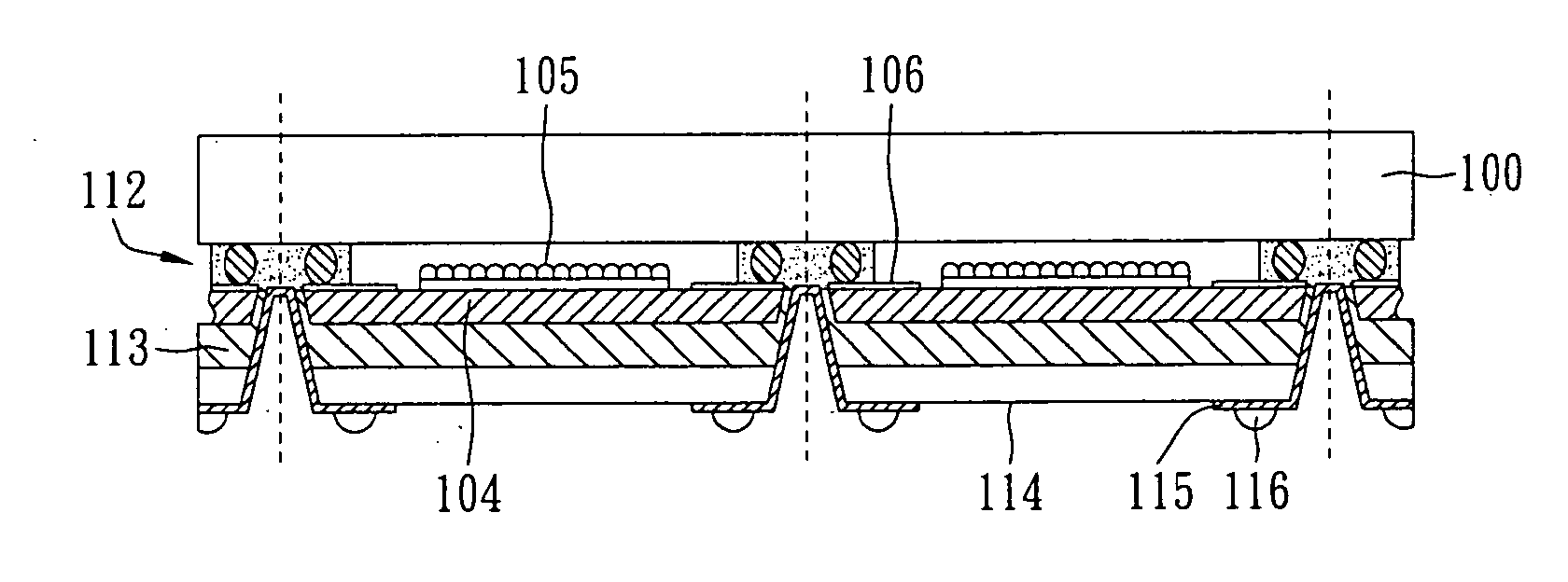
Figure 1 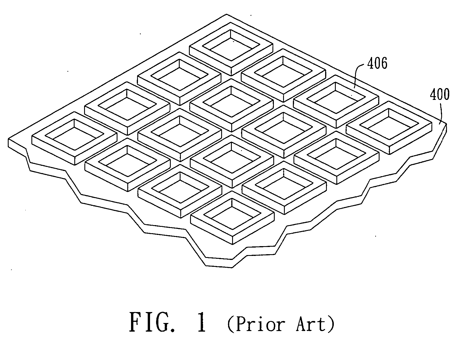
Figure 2 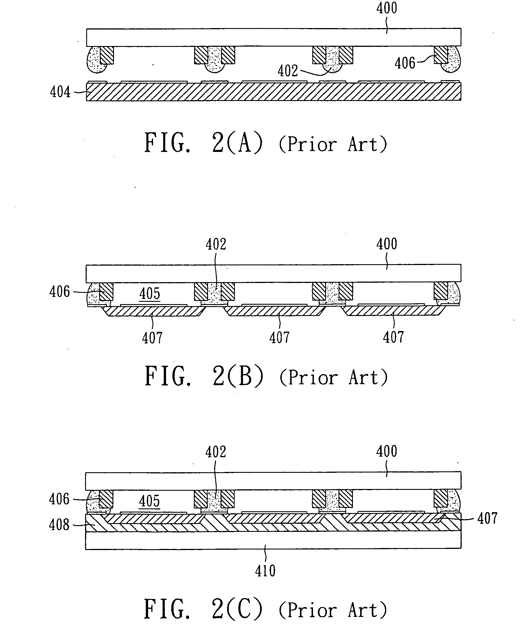
Figure 3
Abstract
Description
BACKGROUND OF THE INVENTION
[0001] 1. Field of the Invention
[0002] This invention relates to an optoelectronic device chip. More particularly, this invention relates to an optoelectronic device chip having a composite spacer structure, and a method for making the optoelectronic device chip having the composite spacer structure.
[0003] 2. Description of the Related Art
[0004] Digital imaging devices have been widely used in many electronic products nowadays. They are used in, for example, digital cameras, digital video recorders, cellular phones with photographing function, safety-control monitors, etc.
[0005] A digital imaging device usually includes an optoelectronic device chip, such as a CCD image sensor chip or a CMOS image sensor chip. Such image sensor chips may be packaged by means of an advanced package technology called “wafer-level chip scale package”, WLCSP. In traditional package technology, a wafer having micro-devices such as electronic devices, electromechanical devi...
Examples
Embodiment Construction
[0025] The present invention will now be described according to its preferred embodiments and drawings. The drawings are for illustrative purpose only; the thickness and width in the drawings are not drawn according to scale.
[0026] FIGS. 3(A)-(C) are cross-sectional views of a preferred embodiment according to the present invention, showing a WLCSP process for making a packaged optoelectronic device chip, such as an image sensor chip. Referring to FIG. 3(A), a device substrate 104 is provided, on which optoelectronic devices 105 such as image sensors have been made. A plurality of conductive pads 106 are provided adjacent to the devices 105. The size of the conductive pads may be designed according to circuit or process requirements. The devices 105 and the conductive pads 106 may be made onto the substrate by, e.g., a CMOS process. A transparent upper substrate 100, serving as an upper package layer, is placed over the device substrate 104. As shown in the drawing, there are a plu...