
Scanning electron microscope with measurement function
a scanning electron microscope and function technology, applied in the direction of material analysis using wave/particle radiation, semiconductor/solid-state device testing/measurement, instruments, etc., can solve the problems of difficult to check, troublesome to revise and check stored amp data, etc., to achieve efficient and easy measurement
Patent Information
- Authority / Receiving Office
- US · United States
- Patent Type
- Applications(United States)
- Current Assignee / Owner
- Publication Date
- 2008-05-08
- Estimated Expiration
- Not applicable · inactive patent
Smart Images
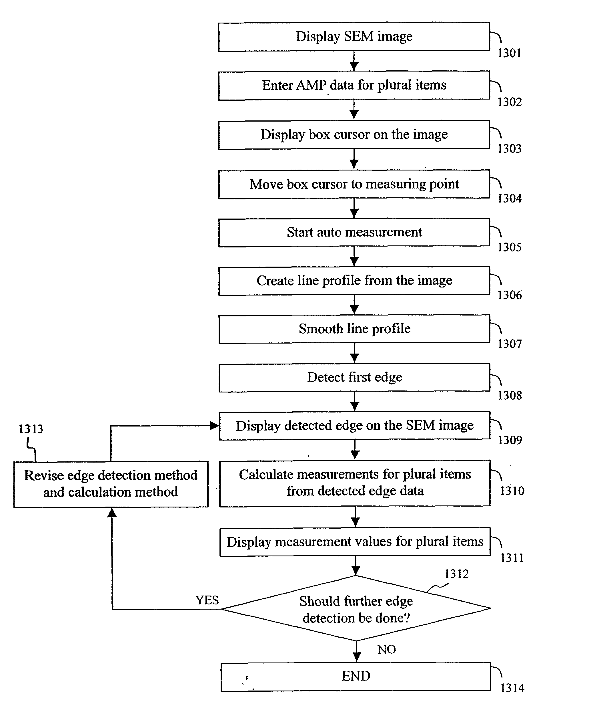
Figure 1 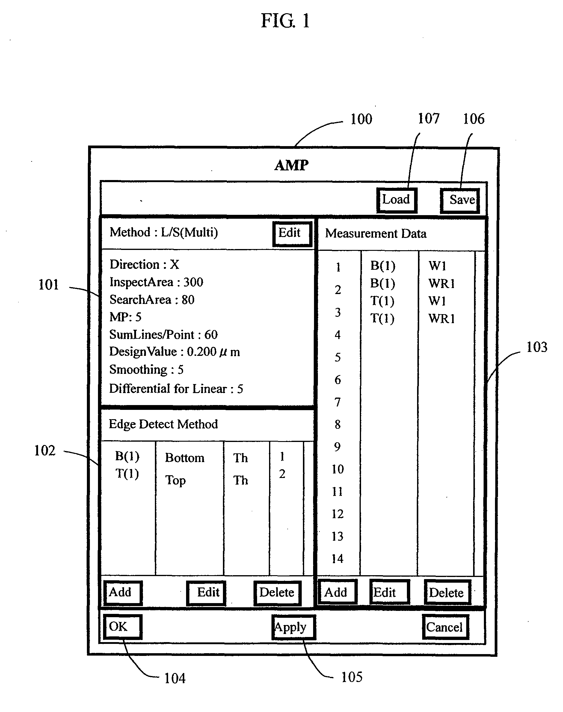
Figure 2 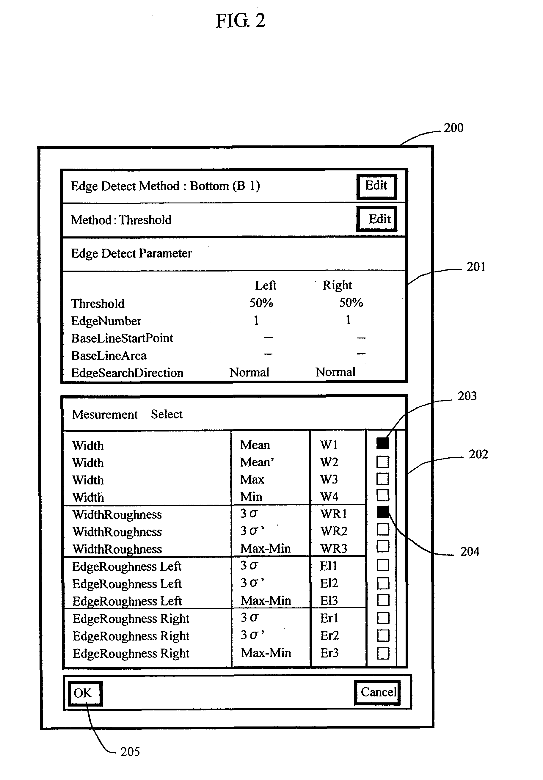
Figure 3
Abstract
Description
CROSS-REFERENCE TO RELATED CASES
[0001] The present application is a continuation of U.S. application Ser. No. 11 / 398,522, filed Apr. 6, 2006, which is a continuation of U.S. application Ser. No. 10 / 779,848, filed Feb. 18, 2004, now U.S. Pat. No. 7,053,371, issued May 30, 2006, which claims the benefit of Japanese Application No. 2003-044290, filed on Feb. 21, 2003, the disclosures of which are herewith incorporated by reference in their entirety.FIELD OF THE INVENTION
[0002] The present invention relates to a scanning electron microscope with a measurement function and a measurement method which uses it. BACKGROUND OF THE INVENTION
[0003] The following patent documents (gazettes) describe conventional techniques in this field:
[0004] Patent Document 1: JP-A No. 347246 / 1994
[0005] Patent Document 2: JP-A No. 22794 / 1996
[0006] Patent Document 3: JP-A No. 237231 / 1999
[0007] Patent Document 4: JP-A No. 213427 / 1998
[0008] Patent Document 5: JP-A No. 201919 / 1999
[0009] A scanning electro...
Examples
Embodiment Construction
[0036] Next, preferred embodiments of the present invention will be described referring to the accompanying drawings.
[0037]FIG. 15 shows the general structure of a scanning electron microscope with a measurement function according to an embodiment of the present invention (see Patent Document 1). An electron beam 2 emitted from an electron gun 1 is narrowed by an objective lens 6 and thrown on a sample 7. The objective lens 6 is excited by an objective lens power supply 11. A deflecting signal generator 14 sends a deflecting signal depending on a scanning area or scanning position of the electron beam 2 as indicated by a computer 21 through a deflecting amplifier 10 to a deflecting coil 5 to excite it so that the sample 7 is scanned with the electron beam 2 two-dimensionally.
[0038] A secondary signal (secondary electron signal, reflection electron signal, etc.), which is generated from the sample 7 in response to irradiation of the electron beam 2, is detected by a detector 12 and...