
Scanning electron microscope with measurement function
a scanning electron microscope and function technology, applied in the direction of instruments, semiconductor/solid-state device testing/measurement, nuclear engineering, etc., can solve the problems of difficult to check, troublesome to revise and check stored amp data, etc., and achieve the effect of efficient and easy measuremen
Patent Information
- Authority / Receiving Office
- US · United States
- Patent Type
- Applications(United States)
- Current Assignee / Owner
- Publication Date
- 2006-10-05
- Estimated Expiration
- Not applicable · inactive patent
Smart Images
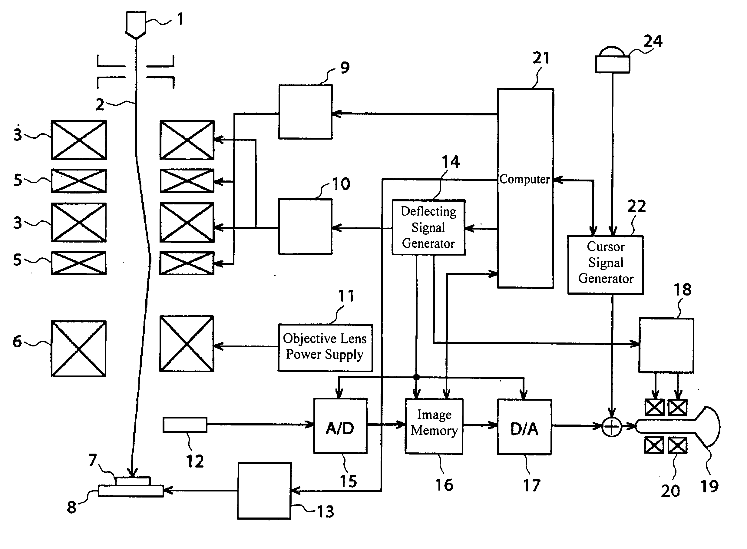
Figure 1 
Figure 2 
Figure 3
Abstract
Description
FIELD OF THE INVENTION
[0001] The present invention relates to a scanning electron microscope with a measurement function and a measurement method which uses it. BACKGROUND OF THE INVENTION
[0002] The following patent documents (gazettes) describe conventional techniques in this field:
[0003] Patent Document 1: JP-A No. 347246 / 1994
[0004] Patent Document 2: JP-A No. 22794 / 1996
[0005] Patent Document 3: JP-A No. 237231 / 1999
[0006] Patent Document 4: JP-A No. 213427 / 1998
[0007] Patent Document 5: JP-A No. 201919 / 1999
[0008] A scanning electron microscope with a measurement function (hereinafter called a measurement SEM) has been used for control of semiconductor sample dimensions or other similar purposes. There are two dimensional measurement modes: a manual measurement mode and an auto measurement mode. In the manual measurement mode, an operator visually makes a measurement using a measurement cursor. In the auto measurement mode, a measurement SEM captures an image of a pattern to...
Examples
Embodiment Construction
[0035] Next, preferred embodiments of the present invention will be described referring to the accompanying drawings.
[0036]FIG. 15 shows the general structure of a scanning electron microscope with a measurement function according to an embodiment of the present invention (see Patent Document 1). An electron beam 2 emitted from an electron gun 1 is narrowed by an objective lens 6 and thrown on a sample 7. The objective lens 6 is excited by an objective lens power supply 11. A deflecting signal generator 14 sends a deflecting signal depending on a scanning area or scanning position of the electron beam 2 as indicated by a computer 21 through a deflecting amplifier 10 to a deflecting coil 5 to excite it so that the sample 7 is scanned with the electron beam 2 two-dimensionally.
[0037] A secondary signal (secondary electron signal, reflection electron signal, etc.), which is generated from the sample 7 in response to irradiation of the electron beam 2, is detected by a detector 12 and...