

Plasma display panel comprising single barrier ribs and double barrier ribs
Patent Information
- Authority / Receiving Office
- US · United States
- Current Assignee / Owner
- Publication Date
- 2008-07-17
- Estimated Expiration
- Not applicable · inactive patent
Smart Images
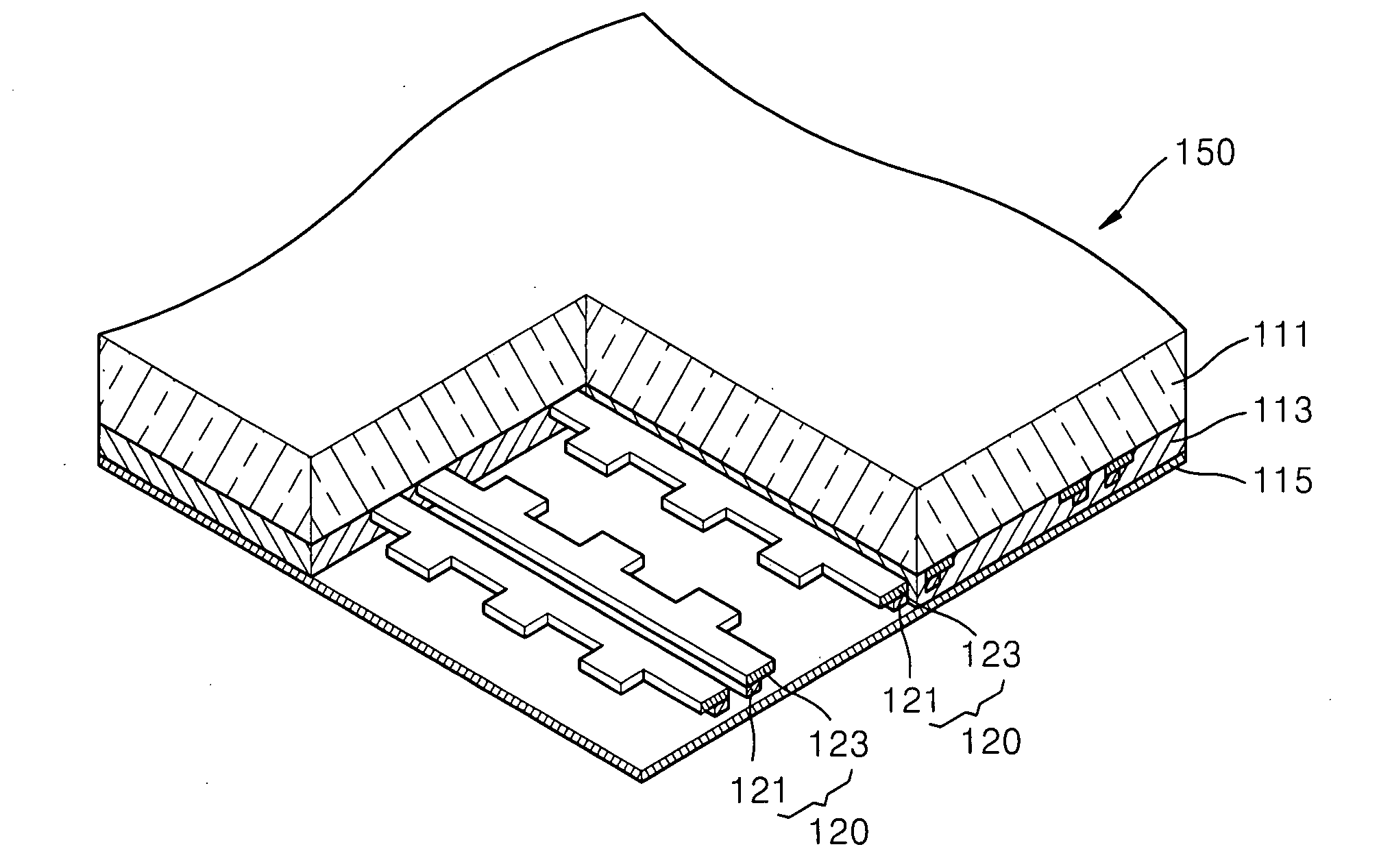
Figure 1 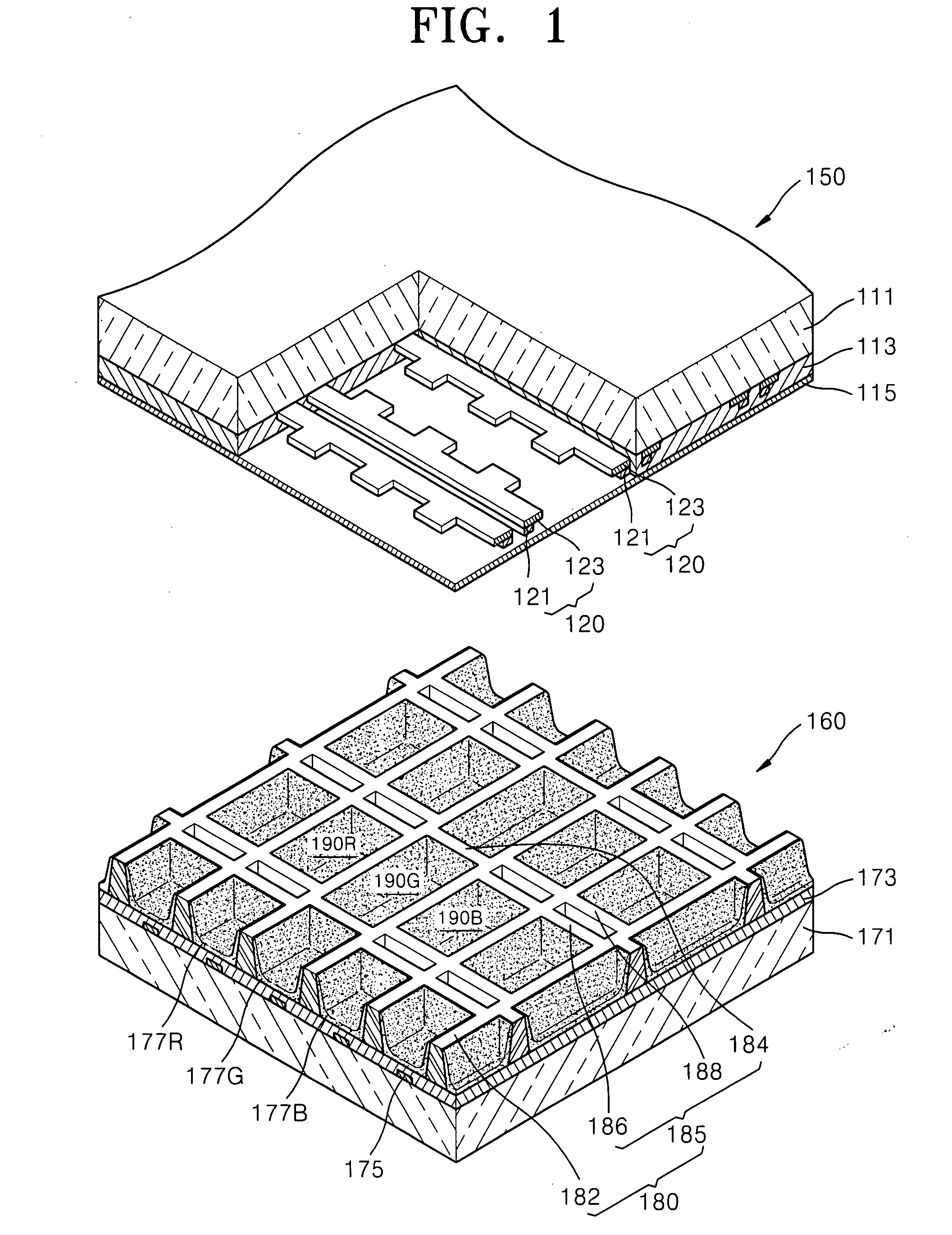
Figure 2 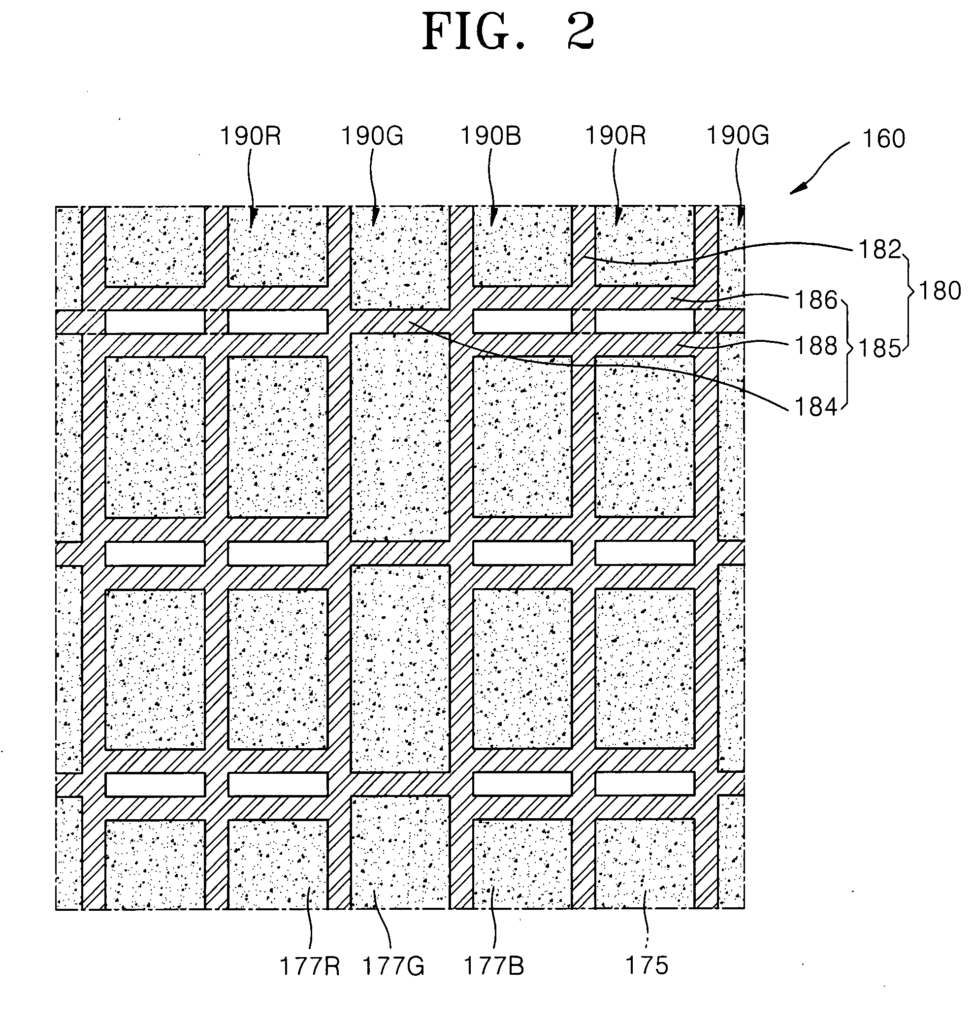
Figure 3
Abstract
Description
CROSS-REFERENCE TO RELATED PATENT APPLICATION
[0001] This application claims the benefit of Korean Patent Application No. 10-2007-0005444, filed on Jan. 17, 2007, in the Korean Intellectual Property Office, the disclosure of which is incorporated herein in its entirety by reference.BACKGROUND OF THE INVENTION
[0002] 1. Field of the Invention
[0003] The present embodiments relate to a plasma display panel including single barrier ribs and double barrier ribs.
[0004] 2. Description of the Related Art
[0005] In general plasma display panels, barrier ribs are arranged between a front panel and a rear panel define a plurality of discharge cells. Also, a phosphor material is coated on the barrier ribs and each of the discharge cells is filled with a main discharge gas, such as Ne, He, or a mixture of Ne and He, and an inert gas including a small amount of xenon (Xe). Such plasma display panels display images by applying a high frequency voltage to the discharge cells to generate vacuum ultraviolet ...
Examples
Embodiment Construction
[0031]The present embodiments will now be described more fully with reference to the accompanying drawings, in which exemplary embodiments are shown.
[0032]FIG. 1 is an exploded perspective view of a plasma display panel according to an embodiment. FIG. 2 is a plan view of a bottom panel 160 of the plasma display panel shown in FIG. 1.
[0033]Referring to FIG. 1, the plasma display panel includes an upper panel 150 and a lower panel 160.
[0034]The upper panel 150 includes an upper substrate 111, a plurality of discharge electrodes 120 arranged parallel to one another on the upper substrate 111, and an upper dielectric layer 113 formed on the upper substrate 111 and covering the discharge electrodes 120. A protection layer 115 is formed on the upper dielectric layer 113.
[0035]The upper substrate 111 may be formed of a highly optical transmissive material, such as glass, as a main component.
[0036]The discharge electrodes 120 include wide transparent electrodes 123 that transmit light, and...