

Light emitting device and electronic appliance
a technology of light emitting devices and electronic appliances, which is applied in the field of oled panels, can solve the problems of reducing the luminance of the oled according, affecting the quality of the final product, and affecting the quality of the final product, and achieves the effect of constant luminan
Patent Information
- Authority / Receiving Office
- US · United States
- Patent Type
- Applications(United States)
- Current Assignee / Owner
- Publication Date
- 2008-08-21
- Estimated Expiration
- Not applicable · inactive patent
Smart Images
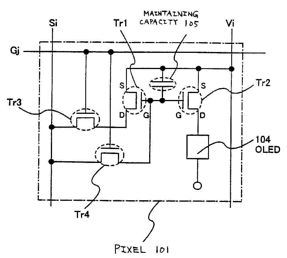
Figure 1 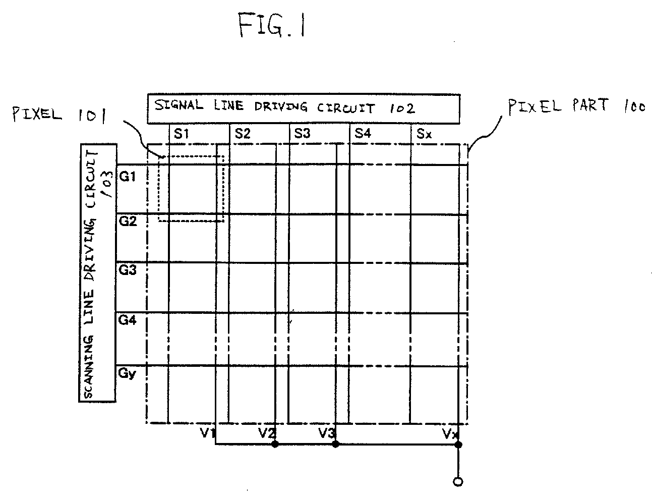
Figure 2 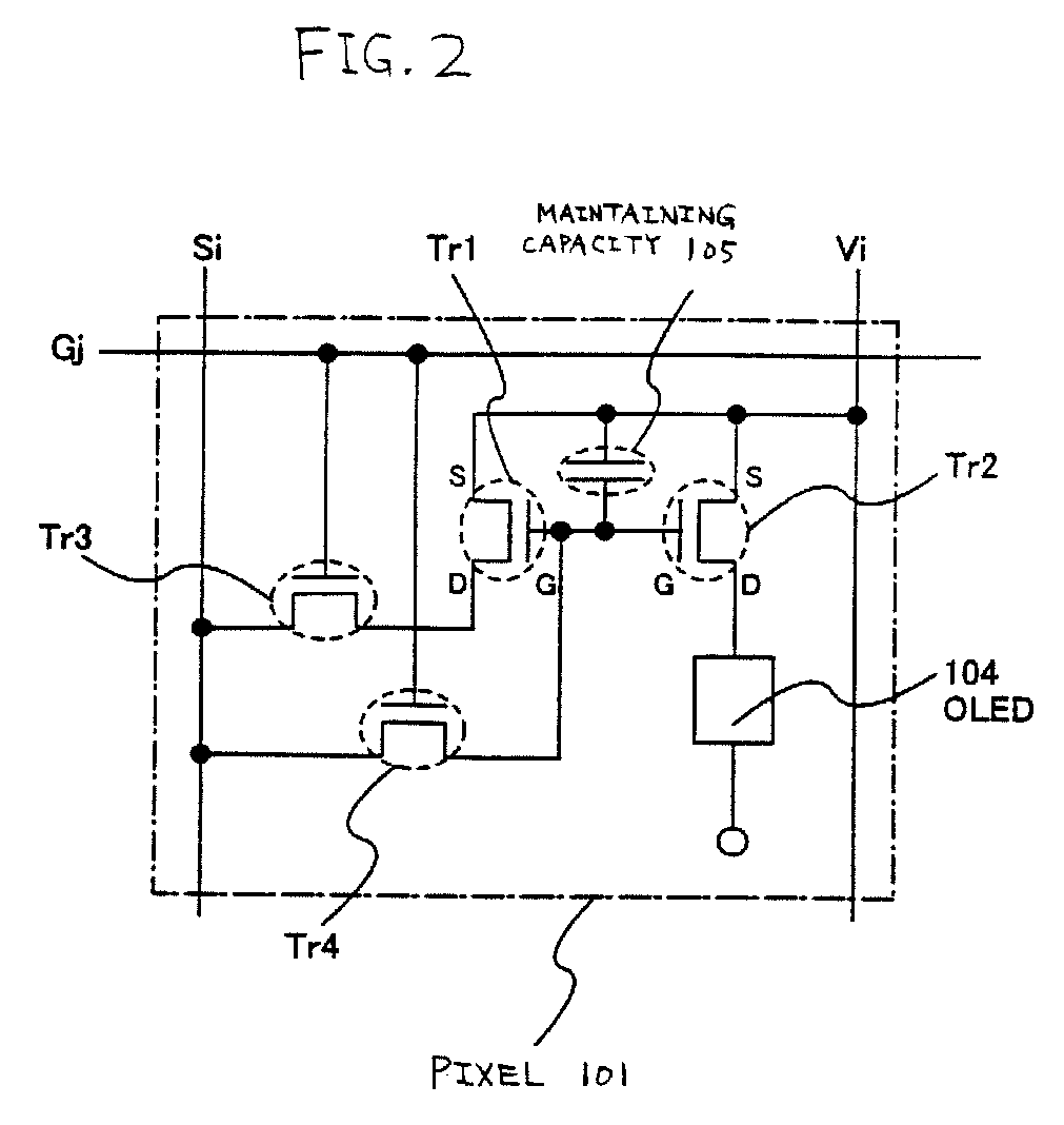
Figure 3
Abstract
Description
BACKGROUND OF THE INVENTION
[0001] 1. Field of the Invention
[0002] The present invention relates to an OLED panel having an organic OLED (OLED: organic light emitting device) formed on a substrate, sealed between the substrate and a cover material. Moreover, it relates to an OLED module having an IC, or the like including a controller packaged on the OLED panel. In this specification, both the OLED panel and the OLED module are referred to as the light emitting device. Furthermore, the present invention relates to an electronic appliance using the light emitting device.
[0003] 2. Description of the Related Art
[0004] The OLED itself emits a light so as to provide a high visibility so that backlighting necessary for a liquid crystal display device (LCD) is not required, and thus it is suitable for providing a thin shape as well as the view angle is not limited. Therefore, recently, a light emitting device using an OLED attracts the attention as the display device for replacing the CRT and t...
Examples
embodiment 1
[0055]FIG. 1 is a block diagram showing the configuration of an OLED panel of the present invention. The numeral 100 is a pixel part, with a plurality of pixels 101 formed in a matrix-like form. Moreover, the numeral 102 is a signal line driving circuit, and the numeral 103 is a scanning line driving circuit.
[0056]Although the signal line driving circuit 102 and the scanning line driving circuit 103 are formed on the same substrate as the pixel part 100 in FIG. 1, the present invention is not limited to the configuration. It is possible that the signal line driving circuit and the scanning line driving circuit 103 are formed on a substrate different from that of the pixel part 100, and connected with the pixel part 100 via a connector such as an FPC. Moreover, although the signal line driving circuit 102 and the scanning line driving circuit 103 are provided one by one in FIG. 1, the present invention is not limited to the configuration. The number of the signal line driving circuit...
embodiment 2
[0095]In this embodiment, a configuration of the pixel 101 shown in FIG. 1 different from that of FIG. 2 will be explained.
[0096]FIG. 7 shows the configuration of the pixel of this embodiment. The pixel 101 shown in FIG. 7 has a signal line Si (one from S1 to Sx), a scanning line Gj (one from G1 to Gy), and a power source line Vi (one from V1 to Vx).
[0097]Moreover, the pixel 101 comprises at least a transistor Tr1 (first current driving transistor), a transistor Tr2 (second current driving transistor), a transistor Tr3 (first switching transistor), a transistor Tr4 (second switching transistor), an OLED 104 and a maintaining capacity 105.
[0098]The gate electrodes of the transistor Tr3 and the transistor Tr4 are both connected with the scanning line Gj.
[0099]One of the source area and the drain area of the transistor Tr3 is connected with the signal line Si, and the other one is connected with the drain area of the transistor Tr1. Moreover, one of the source area and the drain area o...
embodiment 3
[0106]In this embodiment, a configuration of the pixel 101 shown in FIG. 1 different from that of FIG. 2 and FIG. 7 will be explained.
[0107]FIG. 8 shows the configuration of the pixel of this embodiment. The pixel 101 shown in FIG. 8 has a signal line Si (one from S1 to Sx), a scanning line GJ (one from G1 to Gy), and a power source line Vi (one from V1 to Vx).
[0108]Moreover, the pixel 101 comprises at least a transistor Tr1 (first current driving transistor), a transistor Tr2 (second current driving transistor), a transistor Tr3 (first switching transistor), a transistor Tr4 (second switching transistor), an OLED 104 and a maintaining capacity 105.
[0109]The gate electrodes of the transistor Tr3 and the transistor Tr4 are both connected with the scanning line Gj.
[0110]One of the source area and the drain area of the transistor Tr3 is connected with the signal line Si, and the other one is connected with the gate electrode of the transistor Tr1. Moreover, one of the source area and t...