
Dispersion Compensating Varactor Circuit
a varactor circuit and dispersion compensation technology, applied in process and machine control, semiconductor lasers, instruments, etc., can solve the problems of dcf cost, communication signal distortion, and serious second order distortion, and achieve linear delay time compensation, large amplitude rf driving voltage, and easy adjustment
Patent Information
- Authority / Receiving Office
- US · United States
- Current Assignee / Owner
- Publication Date
- 2009-10-01
- Estimated Expiration
- Not applicable · inactive patent
Smart Images
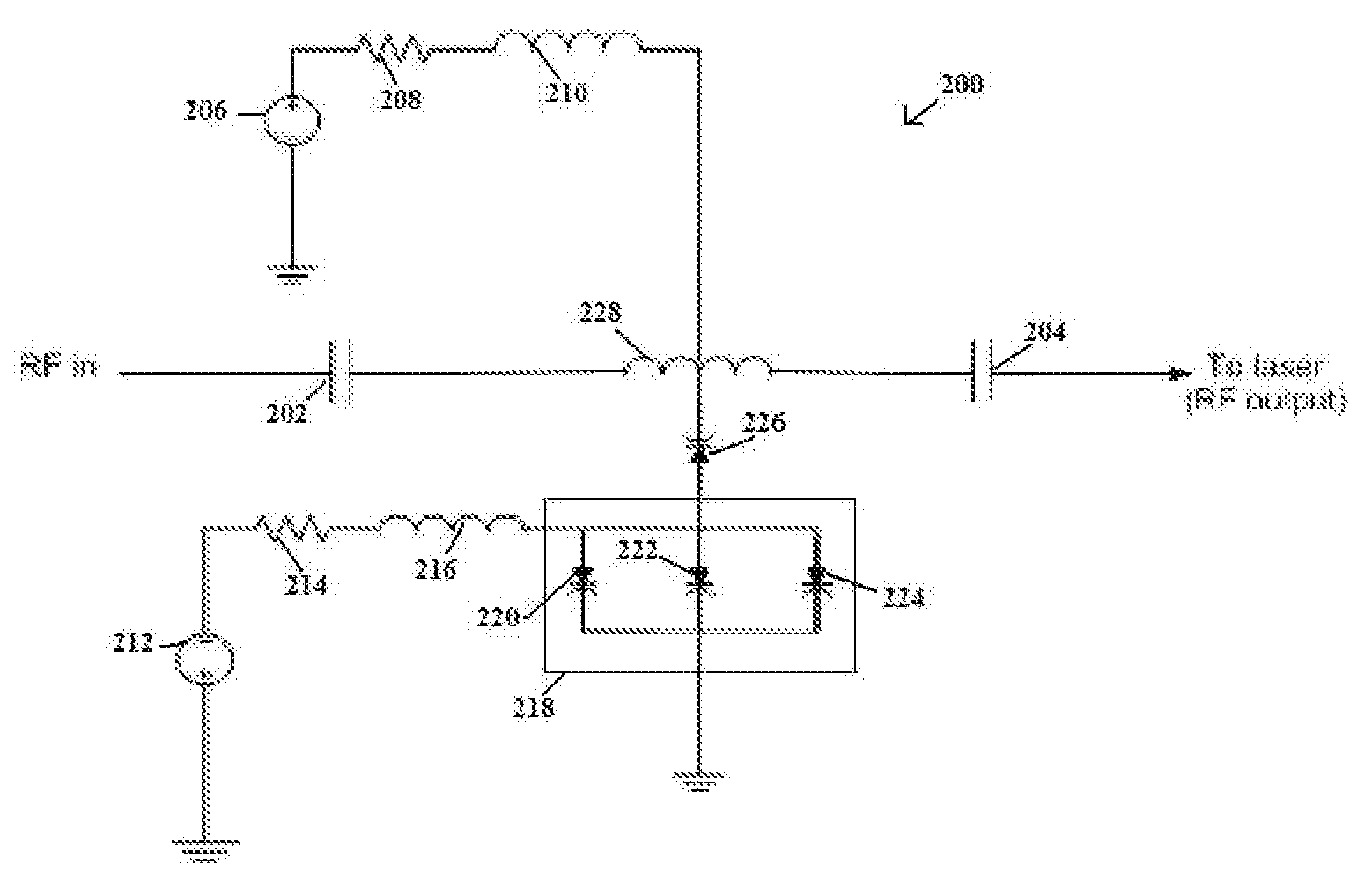
Figure 1 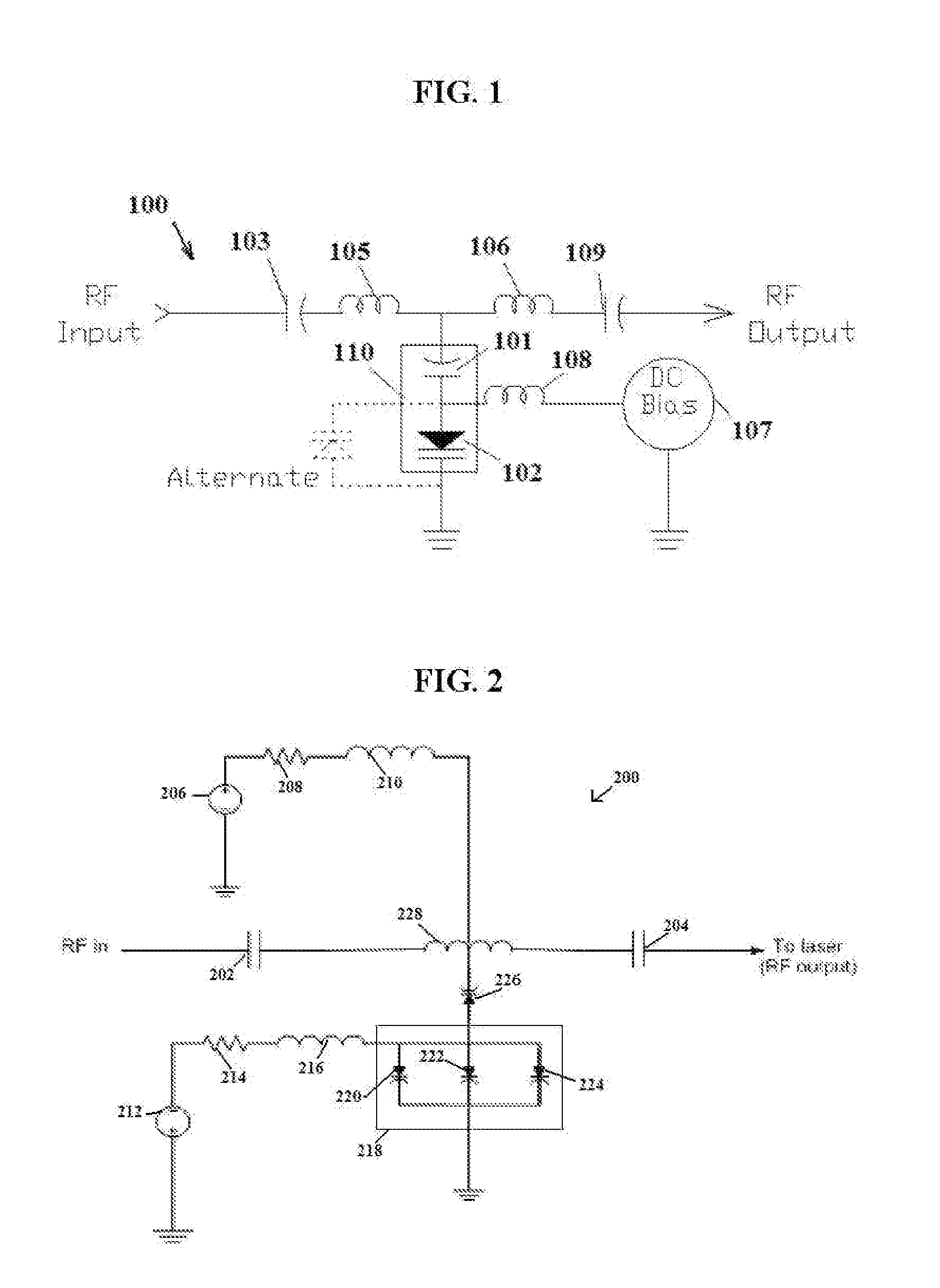
Figure 2 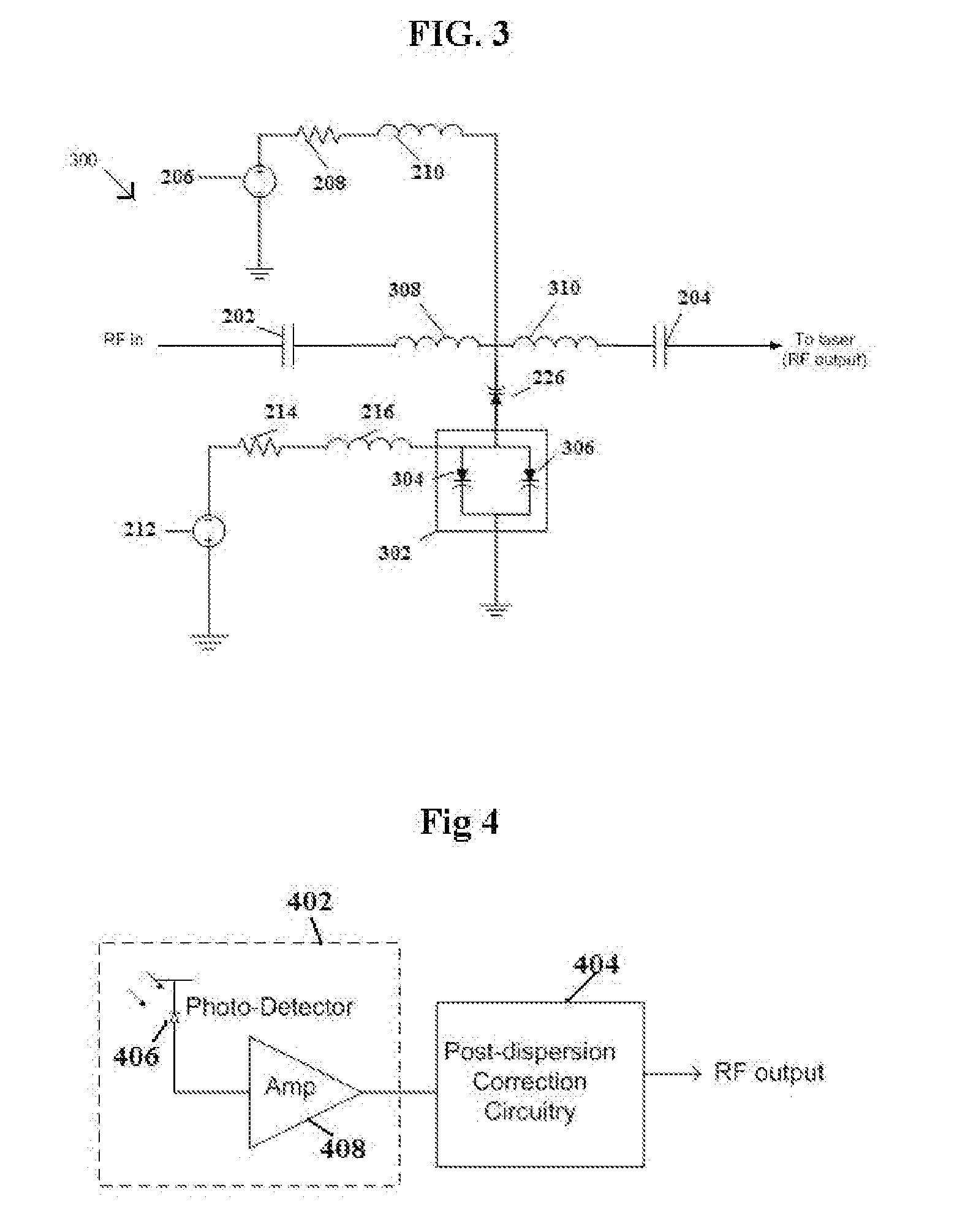
Figure 3
Abstract
Description
BACKGROUND
[0001] 1. Field of the Invention
[0002] The present invention relates to fiber optic transmission systems and dispersion compensating circuits associated with optical transmission systems. In particular the present invention compensates for the laser chirp and chromatic dispersion distortions to enable effective broadband transmission and extended fiber link reach.
[0003] 2. Background of the Invention
[0004] Optical transmission systems are widely used to transmit data on a broadband network. In a typical optical transmission system, a laser provides an optical signal at a predetermined frequency, which is typically modulated to provide an optical transmission data signal.
[0005] In Broadband Passive Optical Network (B-PON) or Gigabit-Passive Optical Network (G-PON) applications, the longest distance is 20 km. So the dispersion compensation needs only to be adequate for fiber lengths up to 20 km.
[0006] In Hybrid Fiber Coaxial (HFC) networks and narrowcast overlay digital applicatio...
Examples
Embodiment Construction
[0032]The capacitance of a varactor at any voltage can be expressed by:
C(V)=Cj0(1−V / Vbi)−γ=Cj1(Vbi−V)−γ, (1)
where Cj1=Cj0(Vbi)−γ. (2)
[0033]Here C(V) is the varactor capacitance at any instant voltage. Cj0 is the varactor capacitance measured at zero voltage. Vbi is the varactor junction voltage. γ is the varactor doping profile parameter. For example, γ=0.5 for an abrupt junction, γ=1 for a hyper-abrupt junction.
[0034]The group delay for the delay-compensating network may be given by:
Tgd=(L1*C(V))1 / 2; (3)
δTgd=(½)*(δC / C)*Tgd. (4)
[0035]Here Tgd is the varactor network delay time, L1 is the inductance in the delay network, and δTgd is the delay time difference selected for the dispersion compensation.
[0036]The RF signal swing at the varactor causes the capacitance of the varactor to change. δC / C is the varactor capacitance change due to the RF voltage swing. The dispersion compensation ability is proportional to the varactor capacitance change δC / C caused by the RF voltage swing.
[0...