
3D integrated circuit device having lower-cost active circuitry layers stacked before higher-cost active circuitry layer
a technology of active circuitry and integrated circuits, which is applied in the field of three-dimensional (3d) integrated circuit devices, can solve the problems of not being able to produce final substrates using general purpose substrate thinning techniques, and not being able to achieve soi circuits having structures,
Patent Information
- Authority / Receiving Office
- US · United States
- Current Assignee / Owner
- Publication Date
- 2010-12-16
Smart Images
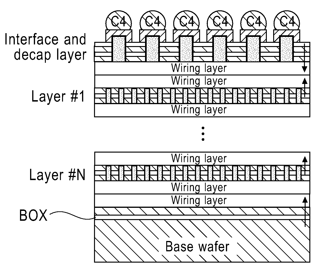
Figure 1 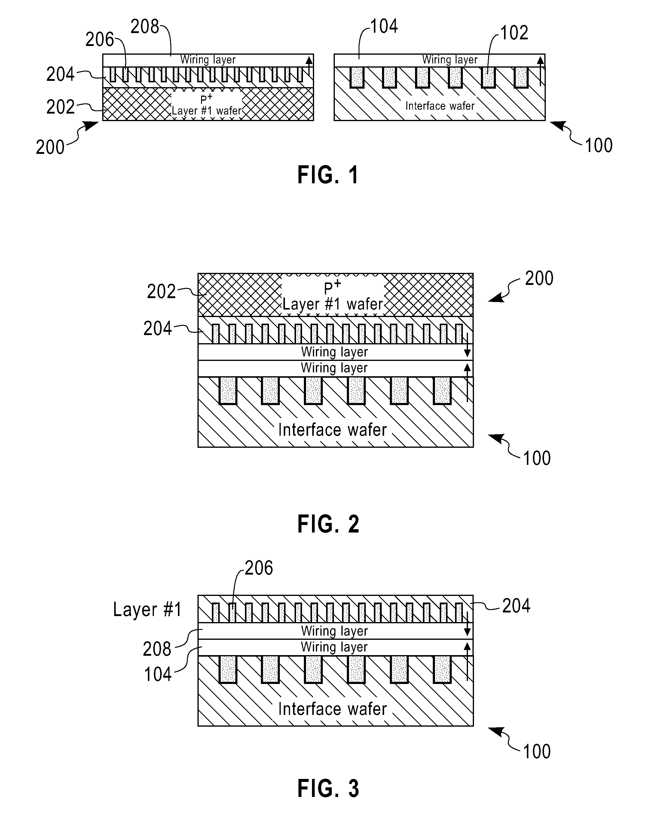
Figure 2 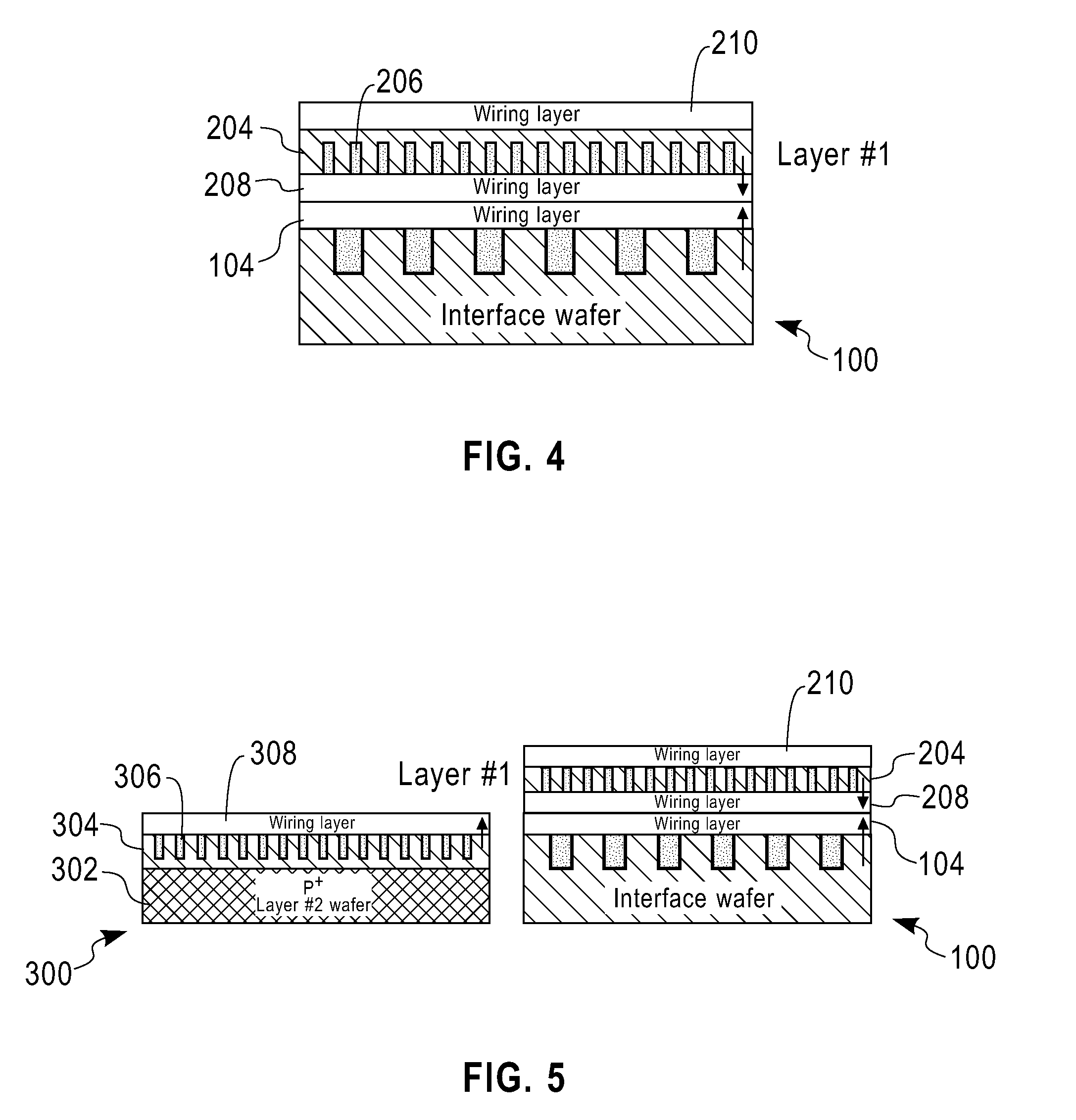
Figure 3
Abstract
Description
CROSS REFERENCE TO RELATED APPLICATIONS
[0001] This application is related to application “3D Integrated Circuit Device Fabrication With Precisely Controllable Substrate Removal,” Ser. No. ______, now ______, and application “3D Integrated Circuit Device Fabrication Using Interface Wafer As Permanent Carrier,” Ser. No. ______, now ______, which were filed on the same day as the present application and commonly assigned therewith to International Business Machines Corporation. These related applications are incorporated herein by reference in their entirety.
[0002] This invention was made with Government support under Contract No.: N66001-04-C-8032 awarded by Defense Advanced Research Projects Agency (DARPA). The Government has certain rights in this invention.FIELD OF THE INVENTION
[0003] The present invention generally relates to the field of integrated circuits, and more particularly relates to the fabrication of three-dimensional (3D) integrated circuit devices.BACKGROUND OF THE INVENT...
Examples
Embodiment Construction
[0017]Preferred embodiments of the present invention will be described in detail hereinbelow with reference to the attached drawings.
[0018]Embodiments of the present invention improve manufacturing yield by stacking lower-cost active circuitry layers of a 3D integrated circuit device before one or more higher-cost active circuitry layers. Lower-cost active circuitry layers are less expensive to manufacture than higher-cost active circuitry layers. In one exemplary embodiment, multiple memory layers of a 3D integrated circuit device are integrated with a logic layer. All of the memory layers are stacked first, and the logic layer is added to the stack last. Because the lower-cost memory layers are stacked before the higher-cost logic layer, the risk of damage to the logic layer during assembly is reduced. Thus, the present invention improves yield for 3D integrated circuit devices, and lowers manufacturing cost.
[0019]FIGS. 1 to 11 illustrate a process for fabricating a three-dimensio...