
Radio frequency directional coupler device and related methods
a technology of radio frequency and coupler, applied in the field of communication, can solve the problems of reducing the directivity of the device, affecting unable to meet the overall desired operating band, so as to improve the bandwidth and directivity, and reduce the number of components
Patent Information
- Authority / Receiving Office
- US · United States
- Patent Type
- Applications(United States)
- Current Assignee / Owner
- Publication Date
- 2011-08-25
Smart Images
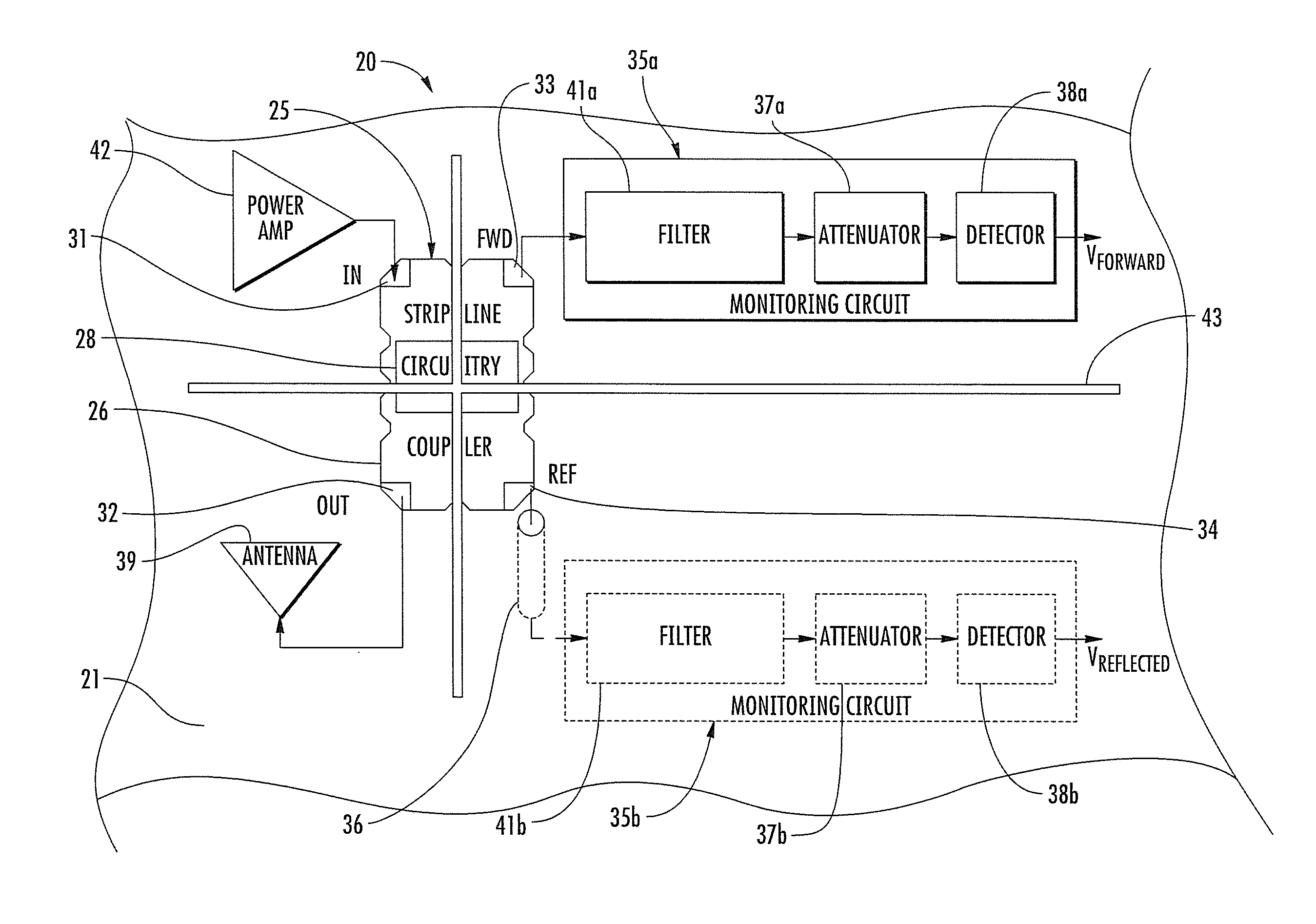
Figure 1 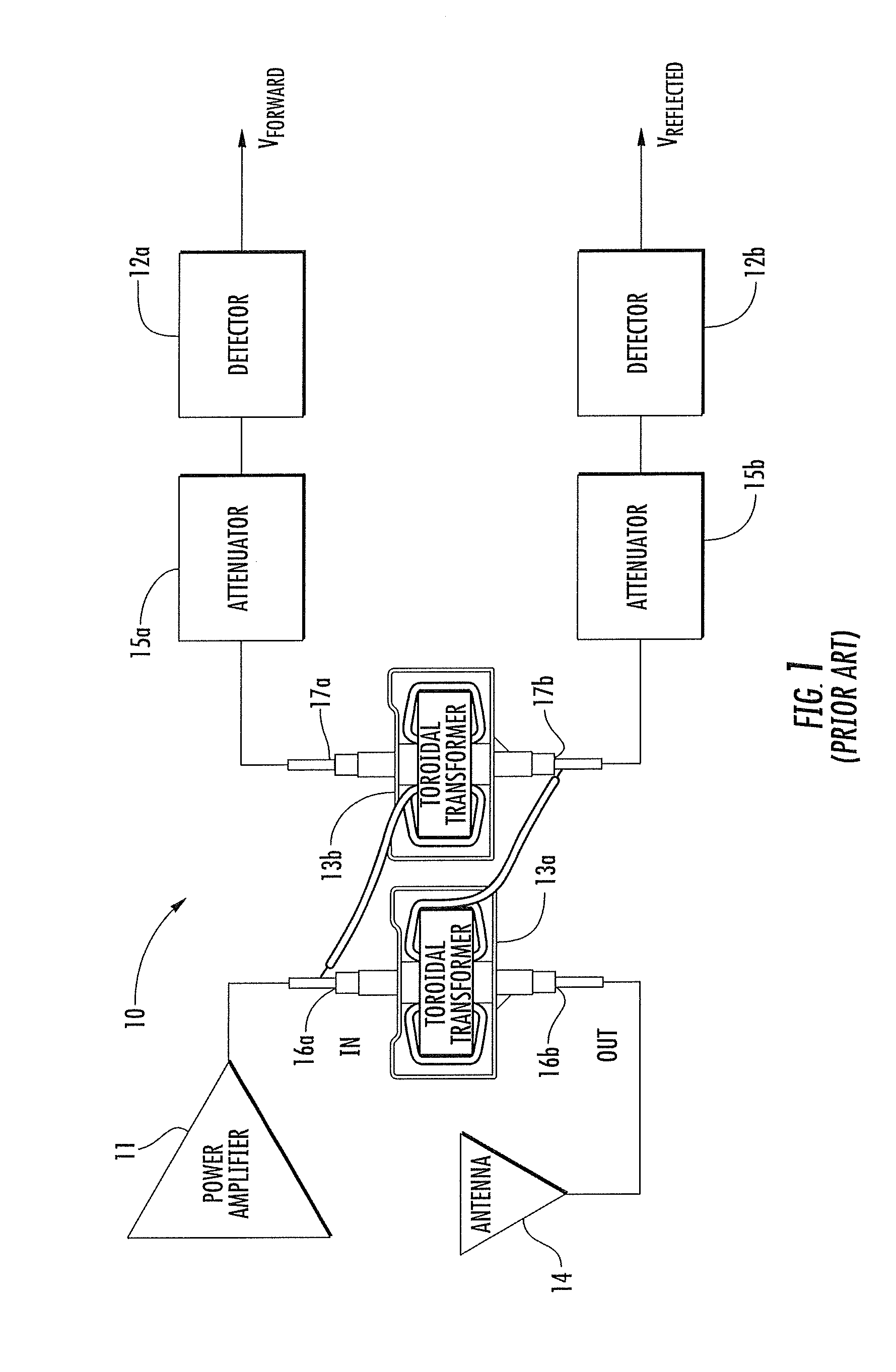
Figure 2 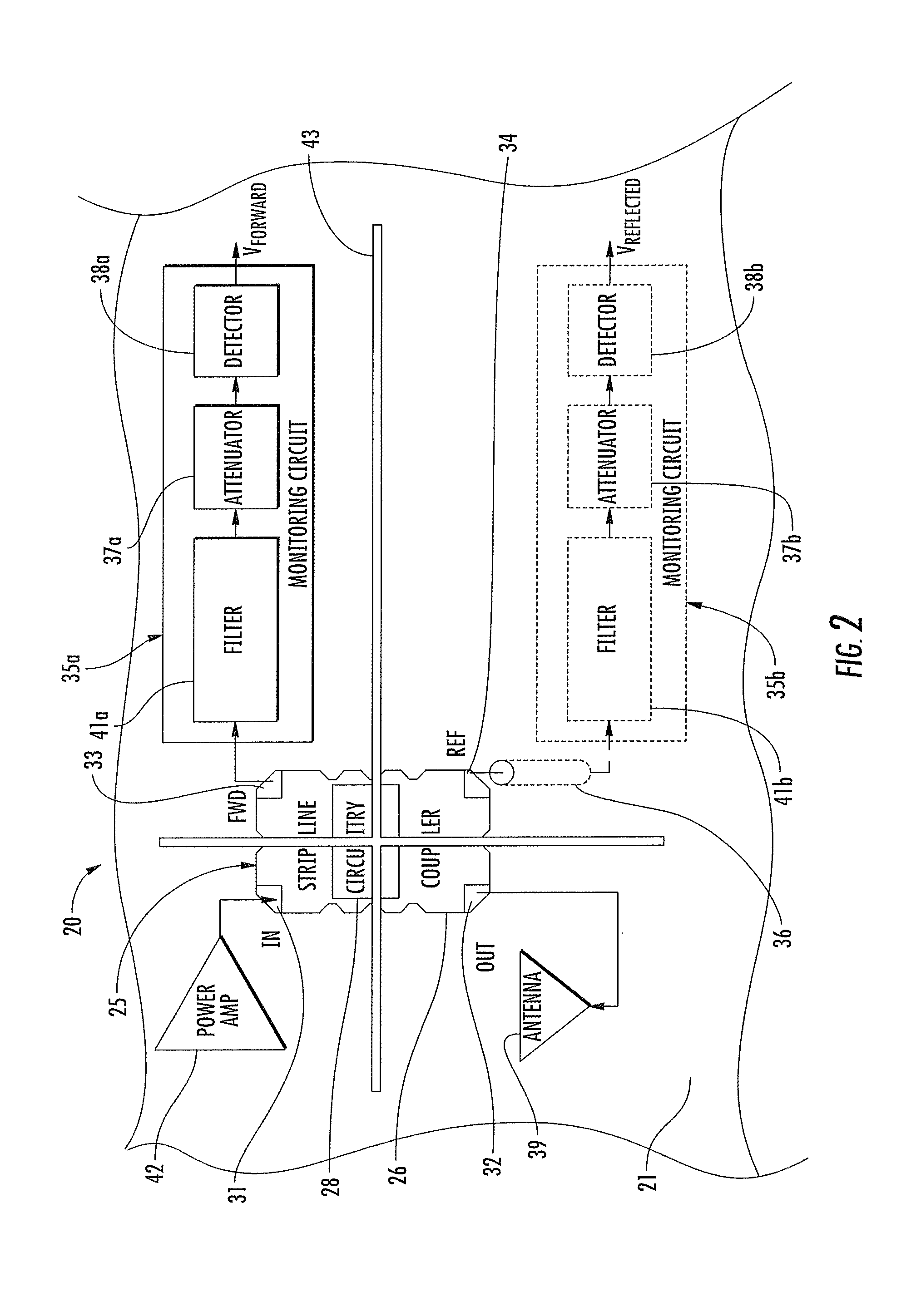
Figure 3
Abstract
Description
FIELD OF THE INVENTION
[0001] The present invention relates to the field of communications and, more particularly, to radio frequency couplers and related methods.BACKGROUND OF THE INVENTION
[0002] A typical broadband power amplifier may include a radio frequency (RF) directional coupler. For example, a typical broadband power amplifier may be a multi-octave power amplifier that generally needs a broadband, multi-octave RF directional coupler for transmitter gain control (TGC). The broadband, multi-octave RF directional coupler may also be needed for voltage standing wave ratio (VSWR) detection, and receive (RX) protect detection. For example, a power amplifier covering a frequency range of about 225-2000 MHz covers operating bands where both very high frequency (VHF) and microwave design techniques may be used. However, neither a VHF nor a microwave approach may be sufficient for the overall desired operating band.
[0003] For example, a prior art system, as illustrated in FIG. 1, include...
Examples
Embodiment Construction
[0024]The present invention will now be described more fully hereinafter with reference to the accompanying drawings, in which preferred embodiments of the invention are shown. This invention may, however, be embodied in many different forms and should not be construed as limited to the embodiments set forth herein. Rather, these embodiments are provided so that this disclosure will be thorough and complete, and will fully convey the scope of the invention to those skilled in the art. Like numbers refer to like elements throughout.
[0025]Referring initially to FIGS. 2 and 3, the electronic device 20 illustratively includes a printed circuit board 21 (PCB) including a ground plane 22 sandwiched between two dielectric layers 29a, 29b and having first and second opposing surfaces 23, 24. The ground plane 22 may be a metallic layer within the PCB 21 (FIG. 3), or may be a metallic layer carried by either the first or second opposing surfaces 23, 24. Other ground plane 22 arrangements will...