
Array substrate of display panel
Patent Information
- Authority / Receiving Office
- US · United States
- Current Assignee / Owner
- Publication Date
- 2016-02-25
Smart Images
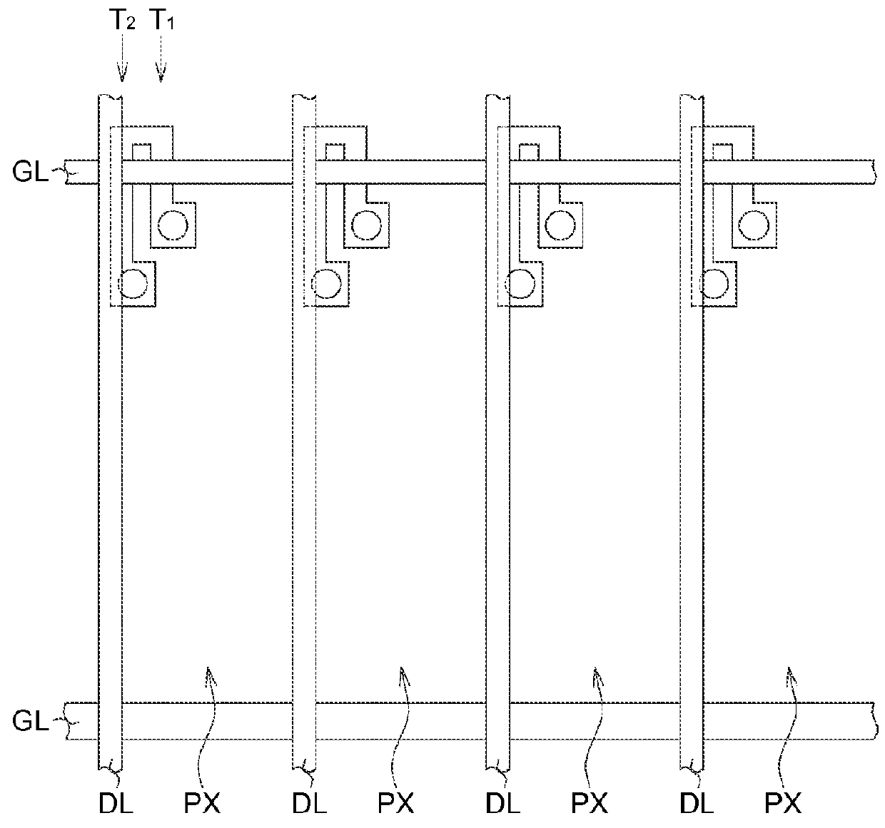
Figure 1 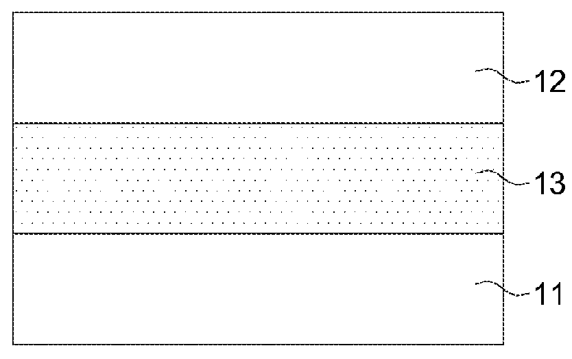
Figure 2 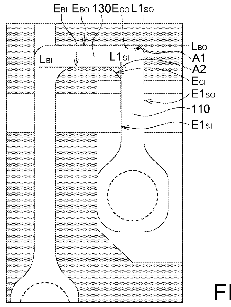
Figure 3
Abstract
Description
[0001] This application claims the benefit of Taiwan application Serial No. 103128987, filed Aug. 22, 2014, the subject matter of which is incorporated herein by reference.BACKGROUND
[0002] 1. Field of the Invention
[0003] The disclosure relates in general to an array substrate of a display panel, and more particularly to an array substrate having a semiconducting layer with different curvatures of the inner and outer edges.
[0004] 2. Description of the Related Art
[0005] Today, electronic products with displays, such as smart phones, tablet personal computers (i.e. tablet PC, flat PC, ex: iPad), laptops, monitors, and televisions, are necessary tools for work and leisure in the daily life. Liquid crystal display (LCD) is the most popular displays in use. Being compact in size, light in weight, power-saving and radiation-free, LCDs are the most popular displays in use. LCD is a flat panel display, electronic visual display, or video display that uses the light modulating properties of liquid...
Examples
first embodiment
[0039]FIG. 5 illustrates a bottom view of another part of the array substrate of a display panel according to the disclosure. The identical elements of FIG. 5 and FIG. 3 are designated with the same reference numerals. According to a LTPS display panel applied with an array substrate of the embodiment, the first transistor T1 has a gate electrode GE, the first lateral portion 110 on the gate electrode GE has a first width W1, and the bottom portion 130 has a second width W2. In one embodiment, the first width W1 is smaller than the second width W2 (W12). It is noted that the applicable embodiment is not limited to the configuration depicted in FIG. 5. In other embodiment, the first width W1 can be larger than the second width W2 (W1>W2). In one embodiment, the turning portion 101 has a third width W3, and the third width W3 is larger than (the first width W12+the second width W22)0.5 (W3>√{square root over (W12+W22)}).
[0040]Moreover, the semiconducting layer 100 comprises an enlargi...
second embodiment
[0043]FIG. 7 illustrates a bottom view of a part of an array substrate of a display panel according to the disclosure. The array substrate of the display panel of the embodiment can be a TFT substrate. The identical elements of FIG. 7 and FIG. 3 are designated with the same reference numerals. Also, it is known that the semiconducting layer 100 is not limited to the U-shaped configuration as depicted in the accompany drawings. The pattern of the semiconducting layer 100 for connecting to the first transistor T1 and the second transistor T2 can be adjusted and altered according to the conditions of the practical applications. The disclosure can be applied to various types of the semiconducting layers having turning portions.
[0044]In the second embodiment, an array substrate similarly comprises a substrate S1, a first transistor T1 and a second transistor T2 disposed on the substrate S1 in series connection. The first transistor T1 and the second transistor T2 are electrically connect...