
Light spot position sensor and displacement measuring device
a technology of displacement measurement and position sensor, which is applied in the direction of converting sensor output optically, instruments, material analysis, etc., can solve the problems of increasing cost and affecting actual precision, and achieve the effect of reducing cos
Patent Information
- Authority / Receiving Office
- US · United States
- Patent Type
- Patents(United States)
- Current Assignee / Owner
- Publication Date
- 2005-01-04
- Estimated Expiration
- Not applicable · inactive patent
Smart Images
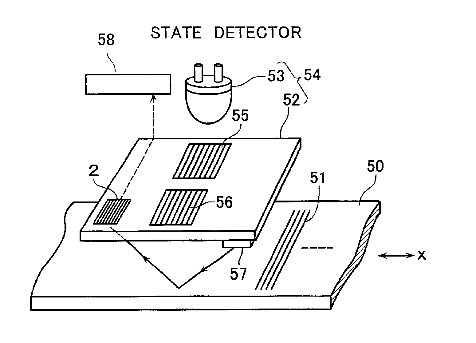
Figure 1 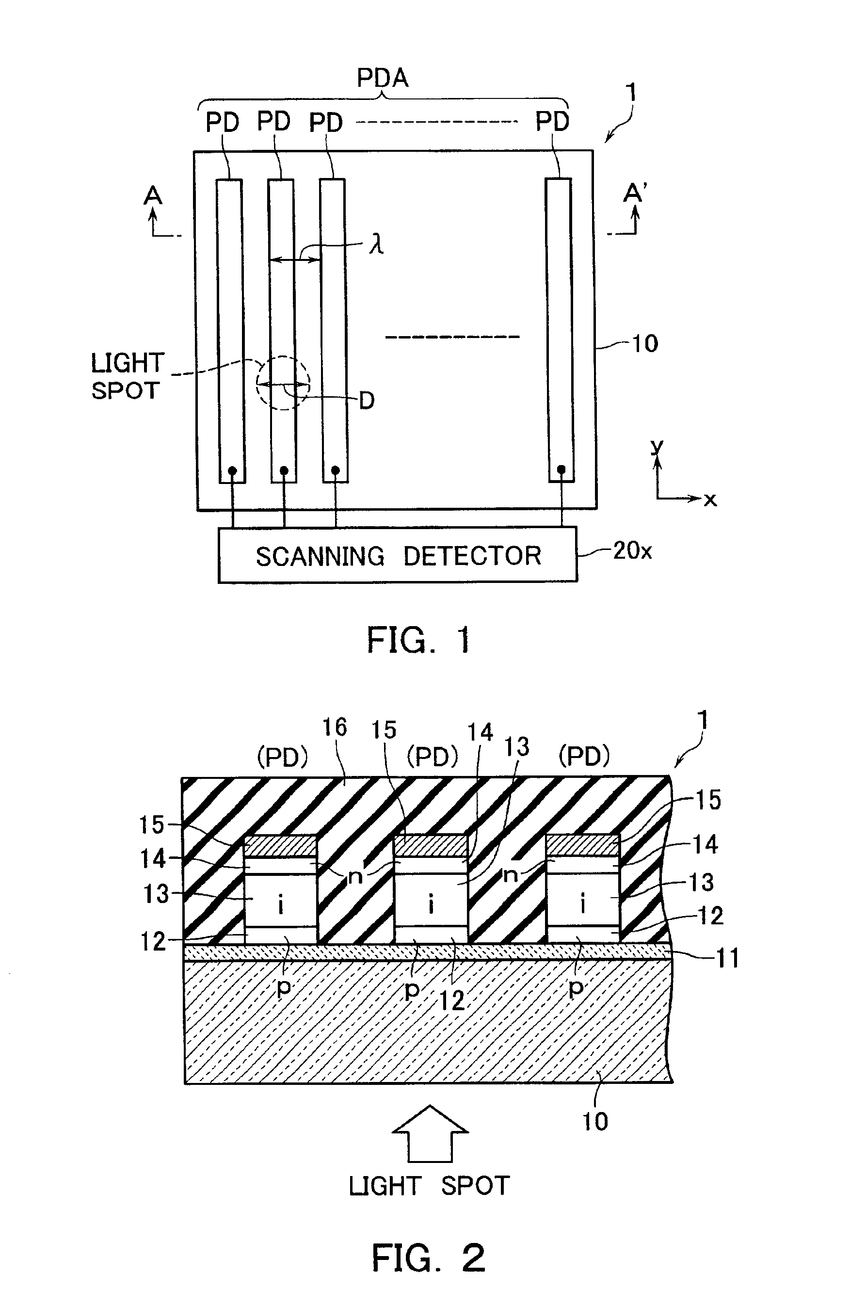
Figure 2 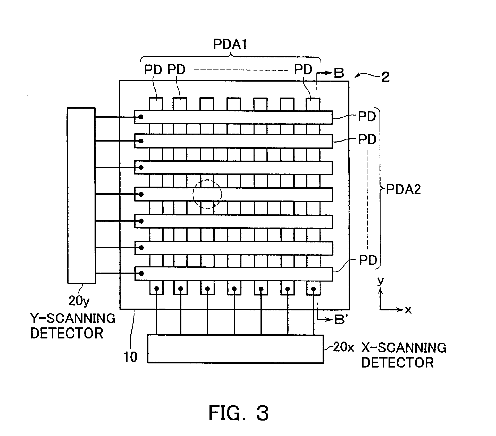
Figure 3
Abstract
Description
BACKGROUND OF THE INVENTION1. Field of the InventionThe present invention relates to a sensor for detecting a light spot position and to a displacement measuring device using the sensor.2. Description of the Related ArtA sensor for detecting an incident position of a light spot can be configured using an existing image sensor such a CCD. Such a light spot position sensor is arranged on one of two members together with a light source for providing a light beam. The light beam output from the light source is reflected at the other of the two members and enters the light spot position sensor. It is theoretically possible to use an incident position of the light beam at this moment to detect a tilt or gap between the two members.There is no actual example of a displacement measuring device that incorporates the above existing CCD. When CCD is incorporated into an encoder part of a small displacement measuring device, a restriction on size causes several disadvantages. For example, the d...
Examples
Embodiment Construction
FIG. 1 is a plan view showing an arrangement of a one-dimensional light spot position sensor 1 for detecting a light spot position and FIG. 2 is a cross-sectional view thereof taken along an A-A′ line. The light spot position sensor 1 comprises a photosensitive device array PDA that includes photosensitive devices (photodiodes) PD shaped in stripes, arrayed along the x-axis and formed on a substrate 10.
The substrate 10 in this embodiment is a transparent substrate such as a glass substrate. A common lower electrode or transparent electrode 11 is formed on the substrate 10. On the transparent electrode 11, amorphous semiconductor layers of p-type 12, i-type 13 and n-type 14 and an upper electrode 15 are deposited in turn. These stacked layers are then patterned to isolate photodiodes PD from each other and array at a certain pitch. A passivation film 16 is formed to cover the photosensitive device array PDA.
The transparent electrode 11 is selected from ITO, SnO2, ZnO and the like. A ...