
Semiconductor device
a semiconductor and memory technology, applied in the direction of diodes, digital storage, radio frequency controlled devices, etc., can solve the problems of numerous problems, thin-film diodes have difficulty in gaining the required on/off ratio, and the structure of memory cells is disclosed, so as to reduce the size of the process, reduce the cell area, and stable cell operations
Patent Information
- Authority / Receiving Office
- US · United States
- Patent Type
- Patents(United States)
- Current Assignee / Owner
- Publication Date
- 2006-08-01
- Estimated Expiration
- Not applicable · inactive patent
Smart Images
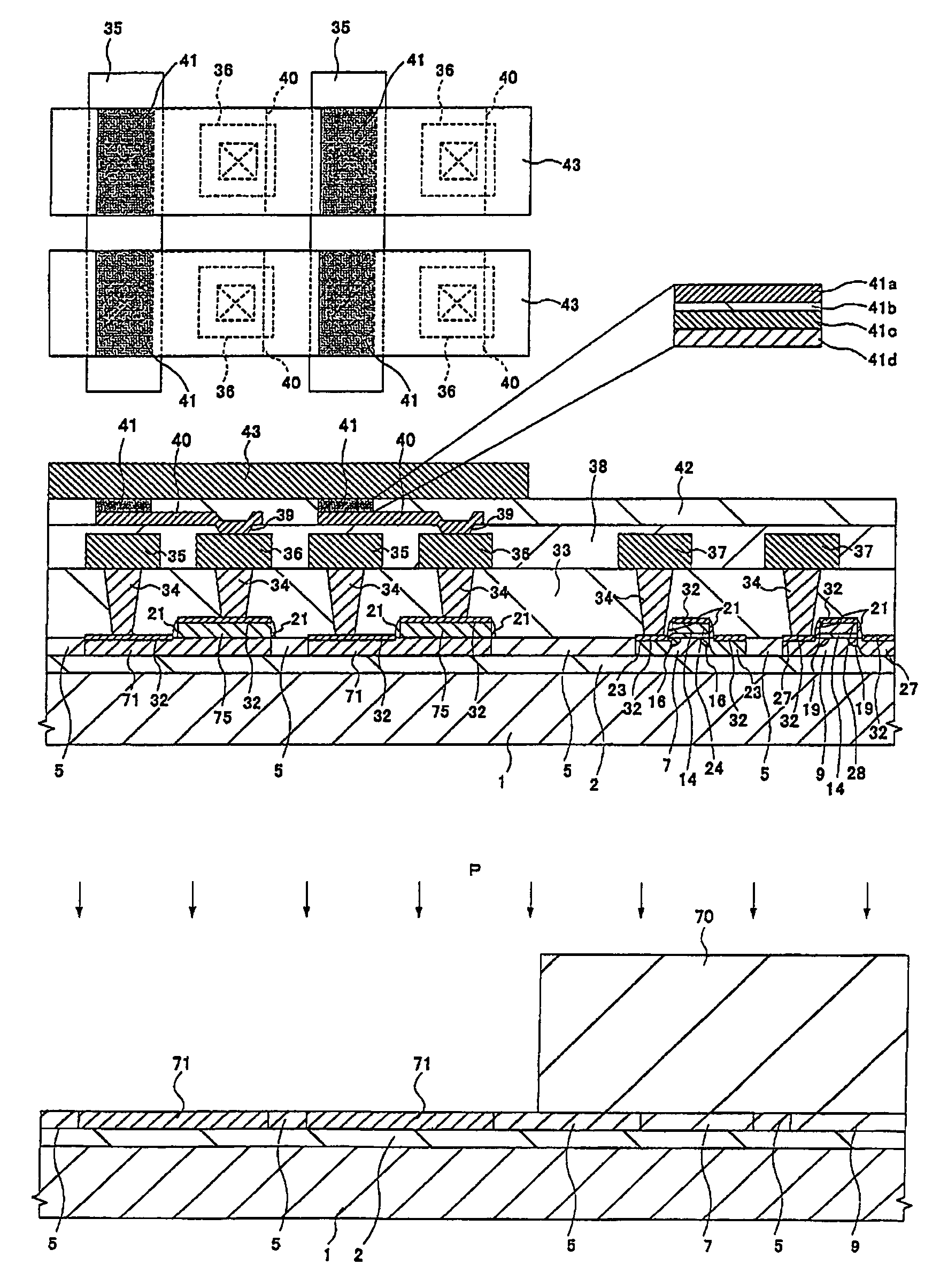
Figure 1 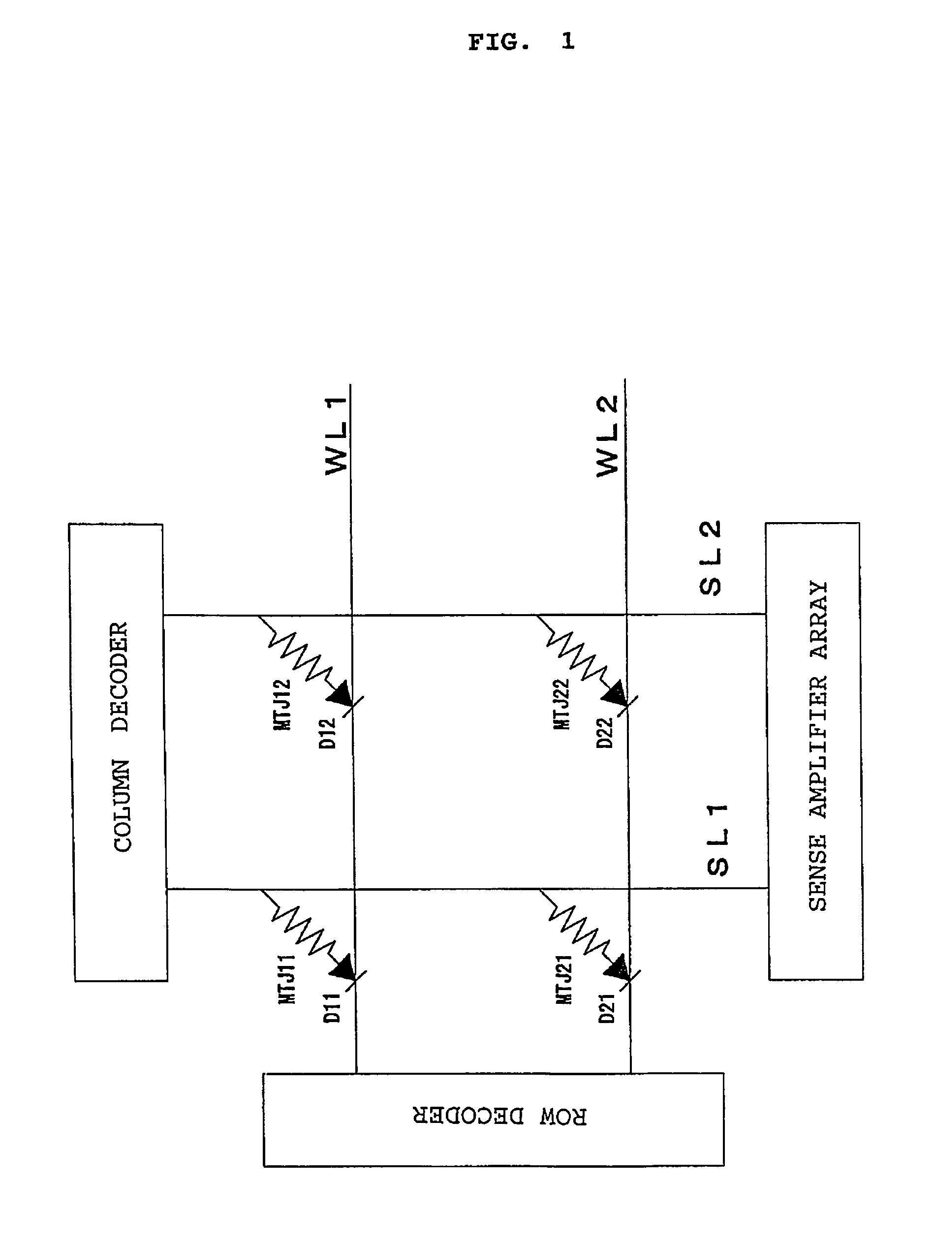
Figure 2 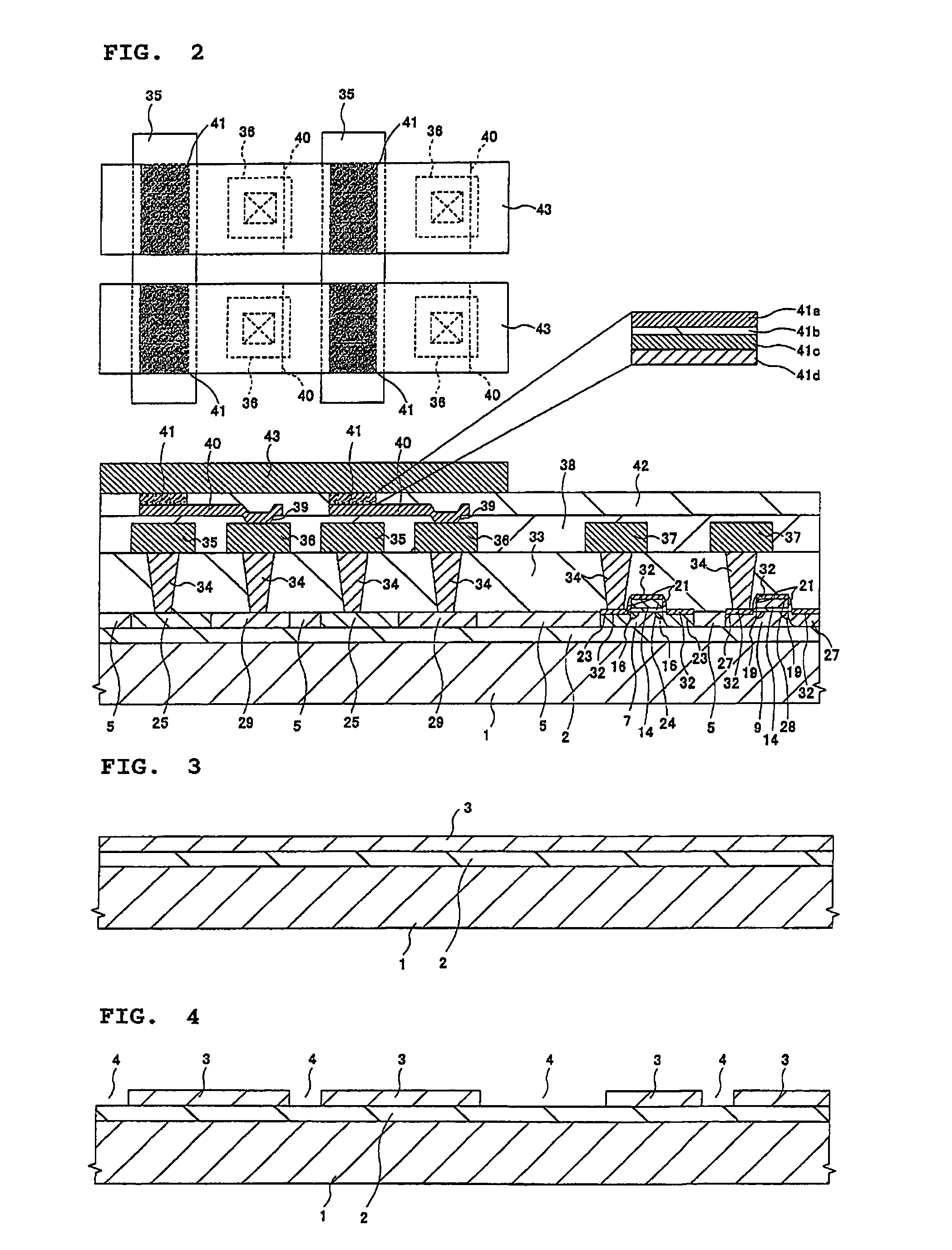
Figure 3
Abstract
Description
[0001] This application is a 371 PCT / JP02 / 11248, Oct. 29, 2002.TECHNICAL FIELD
[0002] The present invention relates to nonvolatile memory devices. More specifically, the present invention relates to technologies to be applied effectively to a memory device adopting a spin valve which utilizes magnetoresistive effects such as a tunnel magnetoresistive effect.BACKGROUND
[0003] A random access memory (RAM) utilizing a magnetoresistive effect, in which a resistance value varies depending on a magnetic orientation, is drawing attention recently. Such a RAM utilizing the magnetoresistive effect is referred to as a magnetoresistive RAM (MRAM). Magnetoresistive effects includes an anisotropic magnetoresistive (AMR) effect, a giant magnetoresistive (GMR) effect, and the like are known. In particular, a tunnel magnetoresistive (TMR) effect, which gains a magnetoresistive effect by use of a tunneling current, is highlighted for capability of gaining large magnetic-field sensitivity.
[0004] A spin-val...
Examples
first embodiment
(First Embodiment)
[0066]FIG. 1 is a circuit diagram showing one example of a memory device (an MRAM) of an embodiment of the present invention, which illustrates partially regarding a memory cell region in particular. As shown in FIG. 1, the MRAM of this embodiment includes word lines WL and sense lines SL. Moreover, magnetic tunnel junction elements MTJ and diodes D are disposed on respective intersecting points of the word line WL and the sense line SL. The magnetic junction element MTJ and the diode D are connected serially to constitute a memory cell. One end (an MTJ end) of the memory cell is connected to the sense line SL and the other end (a D end) thereof is connected to the word line WL. Selection of a memory cell is conducted by selecting one of the sense lines SL and one of the word lines WL, whereby the memory cell located at an intersecting point of the selected sense line SL and the selected word line WL becomes a selected memory cell. Selection of the sense line SL an...
second embodiment
(Second Embodiment)
[0115]An MRAM according to this embodiment is an example of modifying structures of the diodes in the MRAM described in first embodiment. In the following, description regarding the same constitutions as those in first embodiment will be omitted, whereby description will be highlighted on different parts from first embodiment.
[0116]FIG. 24 shows a cross-sectional view and a plan view partially exemplifying a memory cell array and a peripheral circuit on one example of an MRAM according to the second embodiment. The MRAM of this embodiment is formed on a silicon substrate (a silicon wafer) 50. An isolation region 53 is formed on a surface portion of the silicon substrate 50, and a p well 54 and an n well 55 to be defined by the isolation region 53 are formed in a peripheral circuit region. An n-channel-type MOSFET is formed on the p well 54 and a p-channel-type MOSFET is formed on the n well 55. Diodes are formed on the isolation region 53 in a memory cell region. ...
third embodiment
(Third Embodiment)
[0127]An MRAM according to this embodiment is an example of further modifying structures of the diodes in the MRAM described in first embodiment. In the following, description regarding the same constitutions as those in first embodiment will be omitted, whereby description will be highlighted on different parts from first embodiment.
[0128]FIG. 36 shows a cross-sectional view and a plan view partially exemplifying a memory cell array and a peripheral circuit on one example of an MRAM according to the third embodiment. The MRAM of this embodiment is formed on an SOI substrate as similar to the first embodiment. However, the diode of the third embodiment is different from the diode of the first embodiment in that the diode of the third embodiment includes an n-type semiconductor layer 71 generated from a surface semiconductor layer 3 of the SOI substrate, and a p-type semiconductor layer 75 patterned simultaneously with formation of gate electrodes of MOSFETs. In oth...