
Electron source substrate and display apparatus using it
a technology of display apparatus and substrate, which is applied in the direction of instruments, discharge tubes, tubes with screens, etc., can solve the problems of increasing the number of devices damaged by the discharge, affecting the quality of displayed images, and affecting the display apparatus using the conventional sce device described abov
Patent Information
- Authority / Receiving Office
- US · United States
- Patent Type
- Patents(United States)
- Current Assignee / Owner
- Publication Date
- 2006-08-29
- Estimated Expiration
- Not applicable · inactive patent
Smart Images
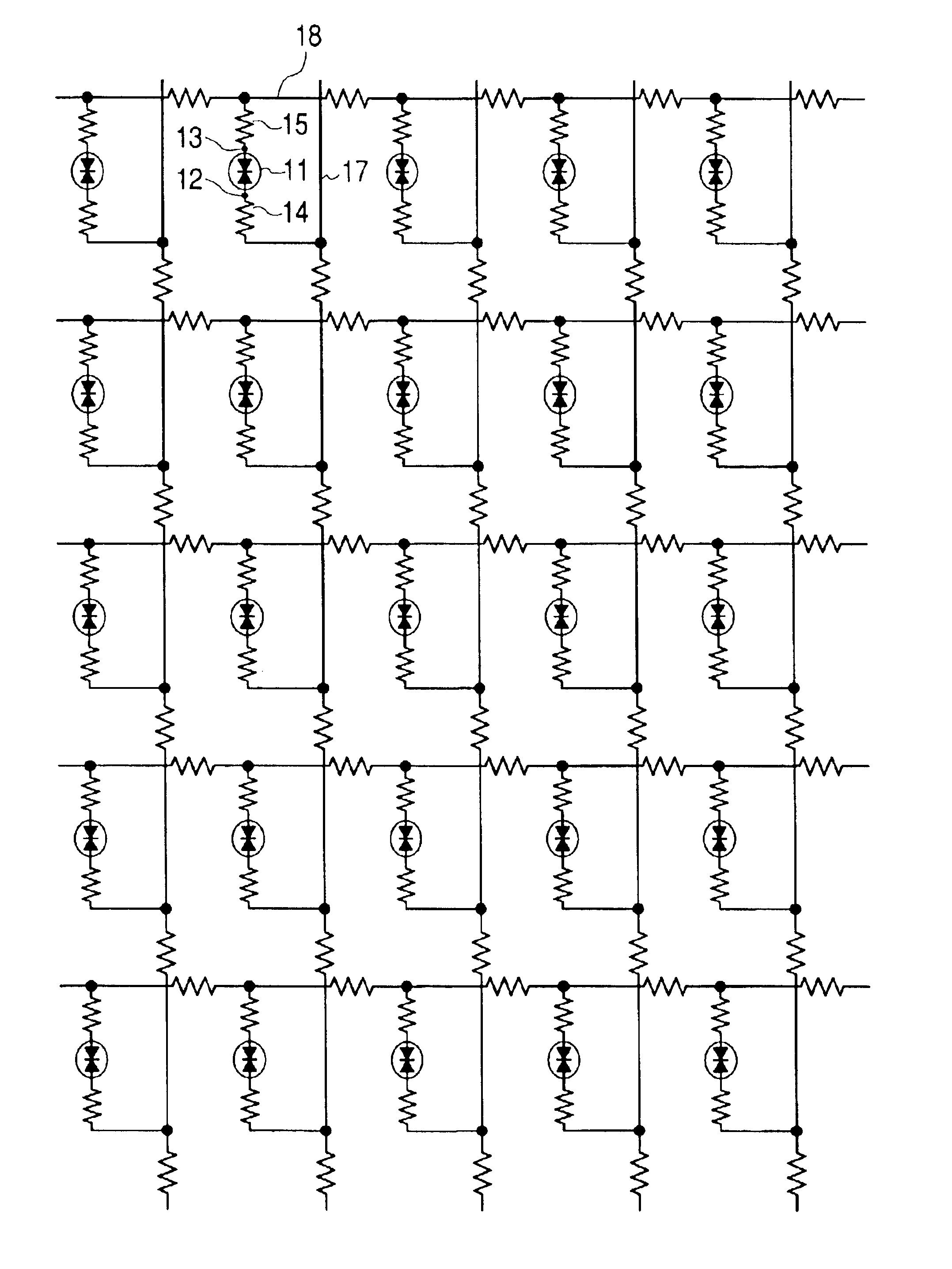
Figure 1 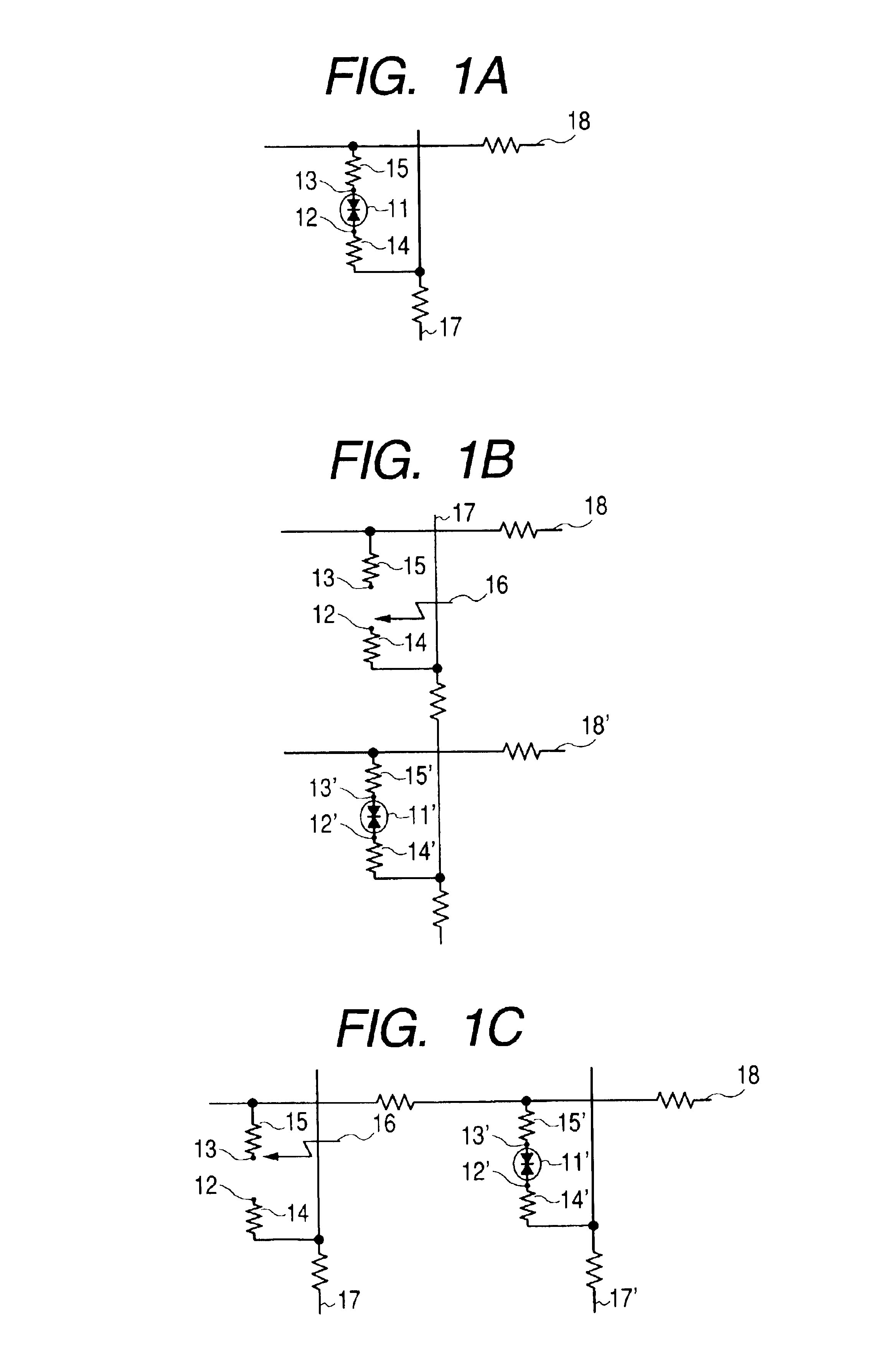
Figure 2 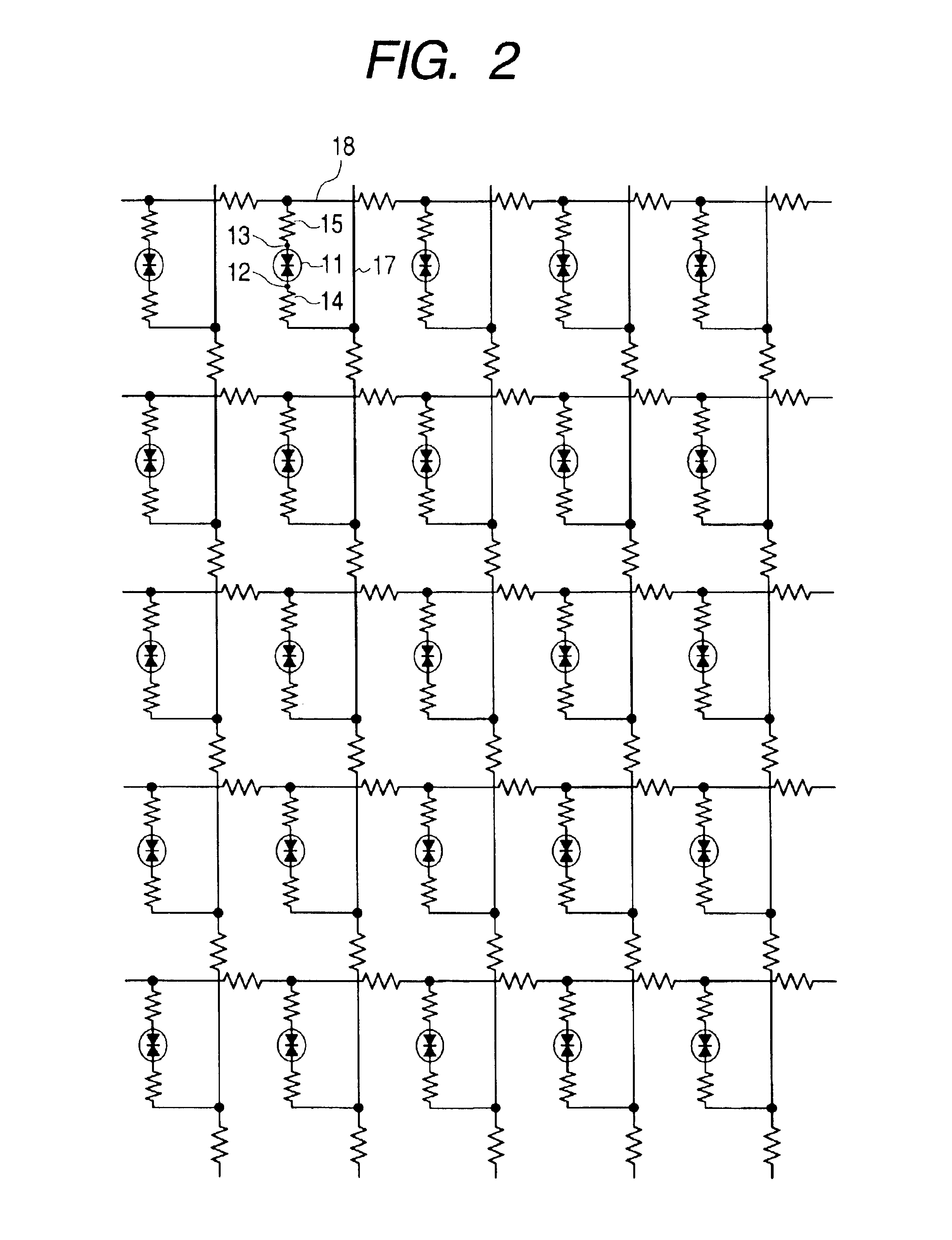
Figure 3
Abstract
Description
BACKGROUND OF THE INVENTION
[0001] 1. Field of the Invention
[0002] The present invention relates to an electron source substrate in which a plurality of electron-emitting devices are arranged in a matrix pattern, and display apparatus using it.
[0003] 2. Related Background Art
[0004] As the electron-emitting devices used in the display apparatus of this type, there are two types of devices: thermal electron sources and cold cathode electron sources. The cold cathode electron sources include field emission devices, metal / insulator / metal devices, surface conduction electron-emitting devices (hereinafter referred to as SCE devices), and so on. The SCE devices will be described herein.
[0005] The SCE devices are devices making use of the phenomenon in which electrons are emitted when an electric current is allowed to flow through a thin film of a small area formed on a substrate and in parallel to the film surface. FIGS. 19A and 19B show the configuration of the M. Hartwell's device as a typical...
Examples
example 1
[0098]FIG. 3 is a schematic diagram showing a schematic configuration of the matrix wiring portion as an example of the electron source substrate according to the present invention. In FIG. 3, the electron-emitting devices 31, paired device electrodes 32, 33, first resistor elements 34, column-directional wiring lines 35, and row-directional wiring lines 36 are similar to those described with the aforementioned equivalent circuit diagram and are formed on the electron source substrate (rear plate) 30. Each electron-emitting device 31 has a pair of device electrodes 32, 33 and a device film is formed so as to connect these device electrodes. The device electrode 33 is coupled to the first resistor element 34, and the device electrode 32 to the second resistor element not shown. The second resistor element is located in a through hole formed in an insulating layer and is thus not shown in FIG. 3.
[0099]A method of producing this rear plate 30 will be described in order. FIGS. 4 to 9 ar...
example 2
[0147]In the present example, the resistor elements are formed only on the column-directional wiring side and the device electrodes also serve as the resistor elements. Specifically, the present example is different from aforementioned Example 1 in that the device electrodes are constructed of resistors, and the other structure is substantially the same as in Example 1. Therefore, only the part of the device electrodes will be described below in detail.
[0148]In the present example, in order to provide the device electrode coupled to the column-directional wiring with a desired resistance, the device electrode is made using a film of mixed materials of a metal and an insulator (which will be referred to hereinafter as a cermet film).
[0149]The metal used in the cermet film in the present example is platinum (Pt) and the insulator is silicon oxide (SiO2). The two materials are processed each into powder, they are mixed each in desired percent by weight, and a sputtering target is fabri...
example 3
[0153]In the present example, an additional resistor element and a specific break line are formed between the column-directional wiring and each device electrode in the configuration of Example 2 described above, and the electron source substrate is constructed in a configuration wherein, with occurrence of large-scale discharge, the specific break line is broken to shut off flow of the discharge current into the other devices more securely. The present example will be described below with FIG. 21.
[0154]FIG. 21 is a schematic configuration diagram (plan view) showing an example of the electron source substrate according to the present invention, which shows only part of the electron source substrate. In FIG. 21, numeral 1001 designates a substrate, 1002 and 1003 device electrodes, 1004 an electroconductive thin film in each device, 1005 an electron-emitting region in each device, 1006 and 1007 column-directional wiring and row-directional wiring coupled to the device electrodes 1002...