
Level shifter
a level shifter and shifter technology, applied in the direction of logic circuit coupling/interface arrangement, pulse technique, instruments, etc., can solve problems such as impossible normal operation
Patent Information
- Authority / Receiving Office
- US · United States
- Patent Type
- Patents(United States)
- Current Assignee / Owner
- Publication Date
- 2008-01-29
- Estimated Expiration
- Not applicable · inactive patent
Smart Images
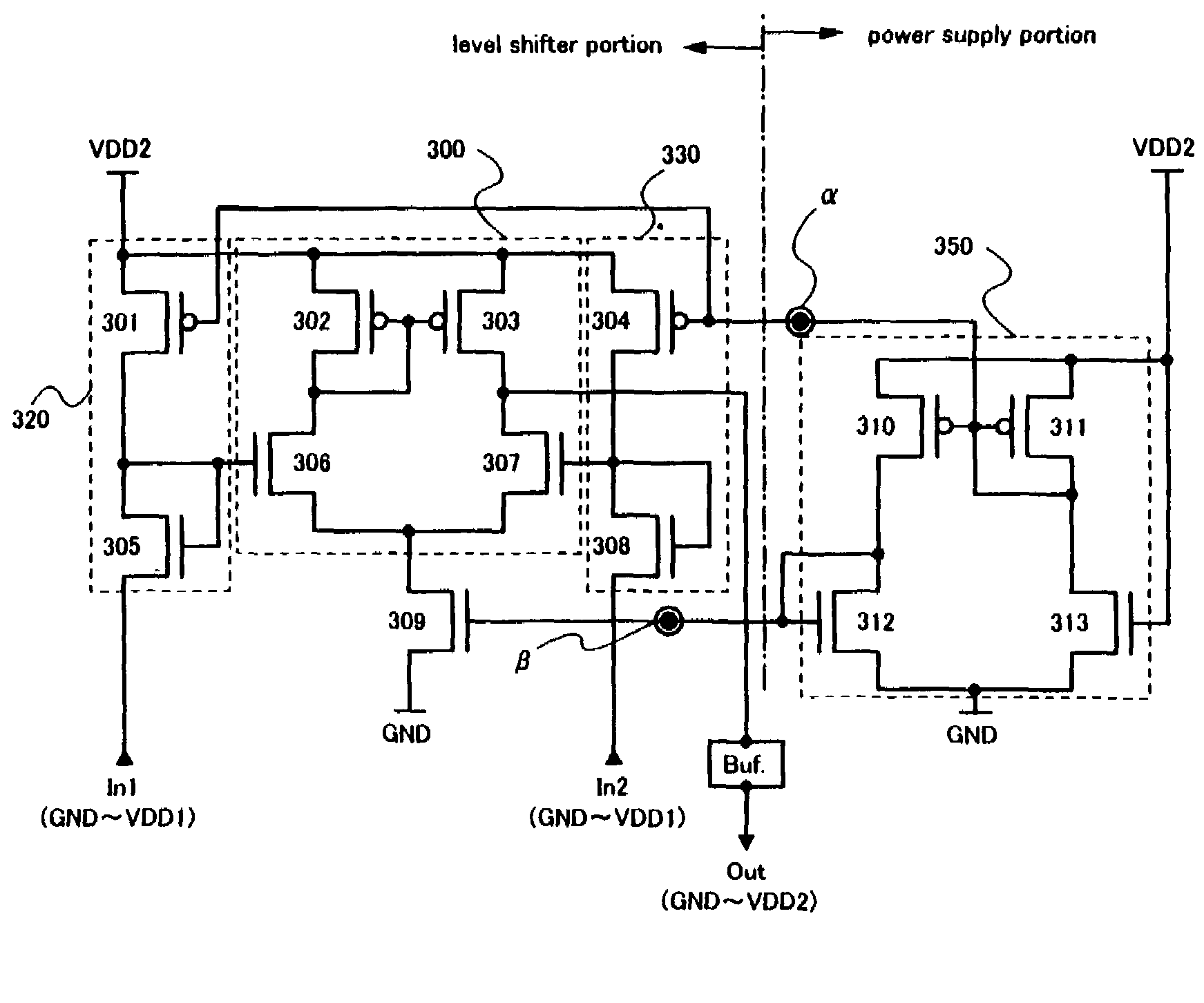
Figure 1 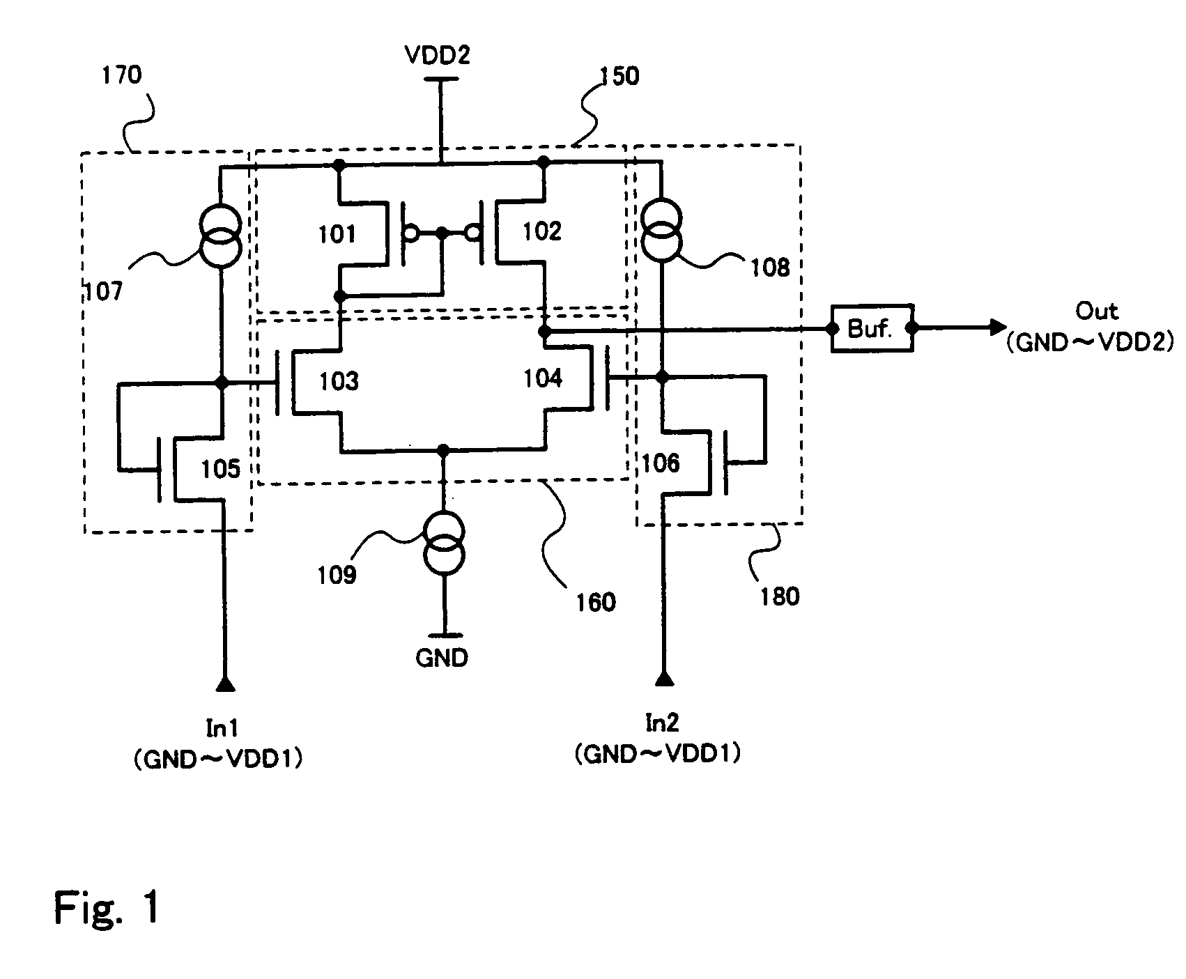
Figure 2 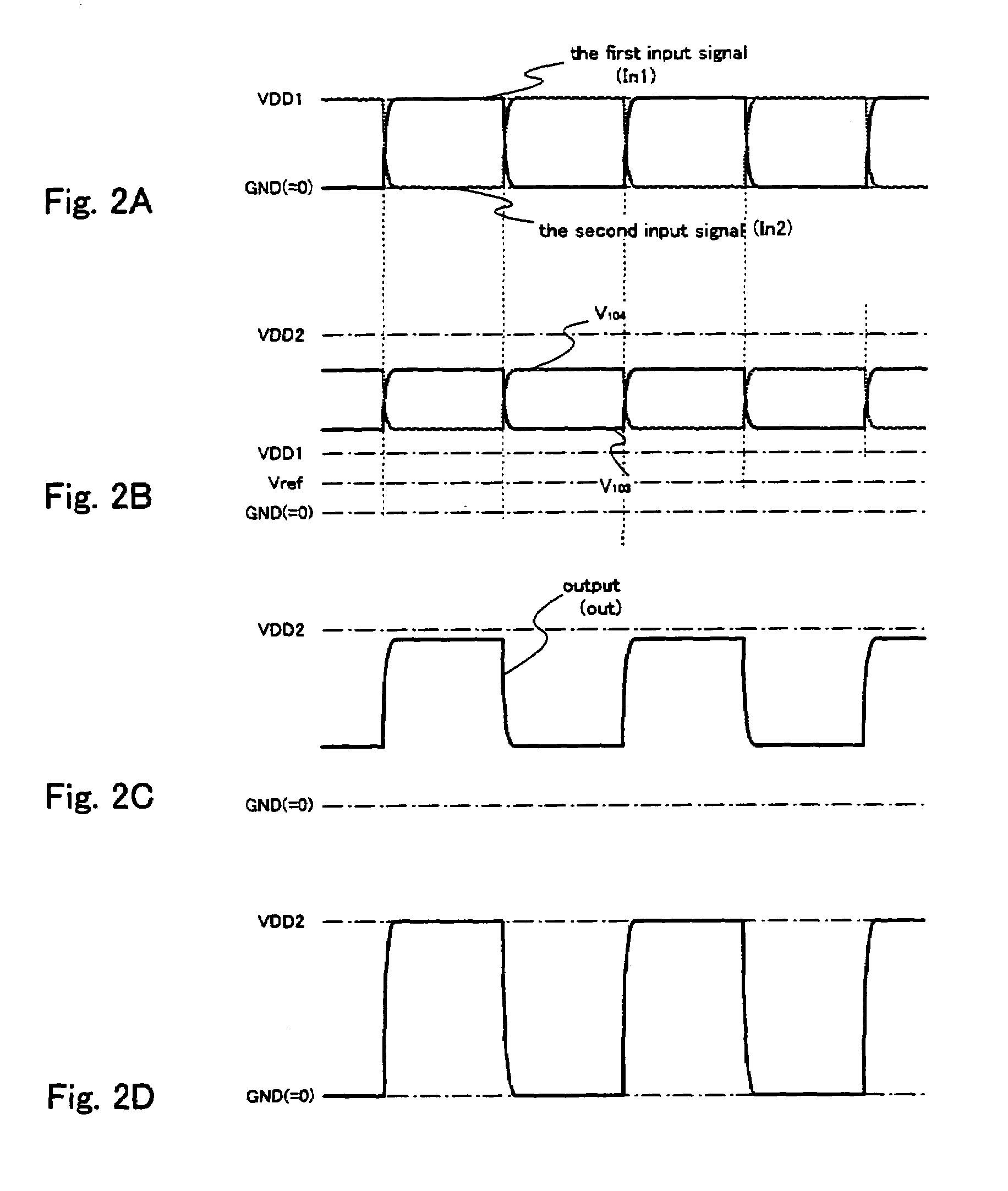
Figure 3
Abstract
Description
[0001] This application is a continuation of U.S. application Ser. No. 09 / 891,560, filed on Jun. 26, 2001 now U.S. Pat. No. 6,731,273BACKGROUND OF THE INVENTION
[0002] 1. Field of the Invention
[0003] The present invention relates to a level shifter used in a driver circuit for a display device, and in particular, to a level shifter used in a driver circuit for a display device, the driver circuit using thin film transistors (hereinafter referred to as TFTs) formed on an insulator. It is to be noted that, in this specification, a display device means one used as an LCD (a liquid crystal display), an OLED (an organic EL display), or the like.
[0004] 2. Description of the Related Art
[0005] Recently, semiconductor microfabrication technology has been advanced, which is accompanied by miniaturization of LSIs. This results in more active application of such LSIs to small-sized apparatus such as personal digital assistants, which requires lower power consumption of such LSIs. Today, LSIs driven a...
Examples
embodiment 1
[0147]FIG. 3 illustrates an embodiment of a level shifter according to the present invention. GND (=0 V), VDD1 (=3 V), and VDD2 (=10 V) are used as power supply potentials in a simulation involved in the description of this embodiment.
[0148]The level shifter of this embodiment is composed of a level shifter portion having a differential amplifier circuit surrounded by a broken line frame 300, a first source follower circuit surrounded by a broken line frame 320, and a second source follower circuit surrounded by a broken line frame 330, and a power supply portion surrounded by a broken line frame 350.
[0149]First, the structure of the power supply portion is described. A source region of a p-type TFT 310, a source region of a p-type TFT 311, and a gate electrode of an n-type TFT 313 are electrically connected to a power supply VDD2. A source region of an n-type TFT 312 and a source region of the n-type TFT 313 are electrically connected to a power supply GND. A drain region of the n-...
embodiment 2
[0159]In Embodiment 1, the amplitude of a signal is converted by fixing the lower voltage side (GND) and converting the higher voltage side from VDD1 to VDD2. In this embodiment, a level shifter structured to convert the amplitude of a signal by fixing the higher voltage side and converting the lower voltage side is described. Here, GND, VDD3, and VDD4 are used as the power potentials in the description wherein VDD433 (=−3 V), and VDD4 (=−10 V) are used as the power supply potentials in a simulation involved in the description of this embodiment.
[0160]FIG. 5 illustrates the structure of a circuit of the level shifter of the present embodiment. The polarities of the TFTs forming the level shifter of the present embodiment are opposite to those of the TFTs forming the level shifter illustrated in FIG. 3. In the present embodiment, a power supply VDD4 is connected at the place where the power supply VDD2 is connected in FIG. 3. This level shifter converts an input signal having the vol...
embodiment 3
[0166]Though each of the level shifters according to the present invention described in Examples 1 and 2 has two input terminals and one output terminal, a level shifter may have one input terminal and one output terminal while using a similar circuit. In this embodiment, a level shifter having one input terminal and one output terminal for converting a signal having the voltage amplitude of GND-VDD1 into a signal having the voltage amplitude of GND-VDD2 is described by way of example.
[0167]FIG. 7 shows an exemplary level shifter having one input terminal and one output terminal. There is no difference in the circuit structure between the level shifter of this embodiment and the level shifter of Embodiment 1 except that the terminal to which the second signal (In2) is input in Embodiment 1 is connected to a power supply Vref in this embodiment. Here, GND (=0 V), VDD1 (=3 V), VDD2 (=10 V), and Vref (=1.5 V) are used as the power supply potentials. It is preferable that the potential ...