
High performance transistors with hybrid crystal orientations
a technology of hybrid crystals and transistors, applied in the field of metal oxide semiconductor field effect transistors (mosfets), can solve the problems of inability to adapt to nfet devices, significant deformation of electron mobilities on (110) si surfaces, and undesirable width of pfets, etc., and achieves less complex fabrication processes and more scalable effects
Patent Information
- Authority / Receiving Office
- US · United States
- Patent Type
- Patents(United States)
- Current Assignee / Owner
- Publication Date
- 2009-11-03
- Estimated Expiration
- Not applicable · inactive patent
Smart Images
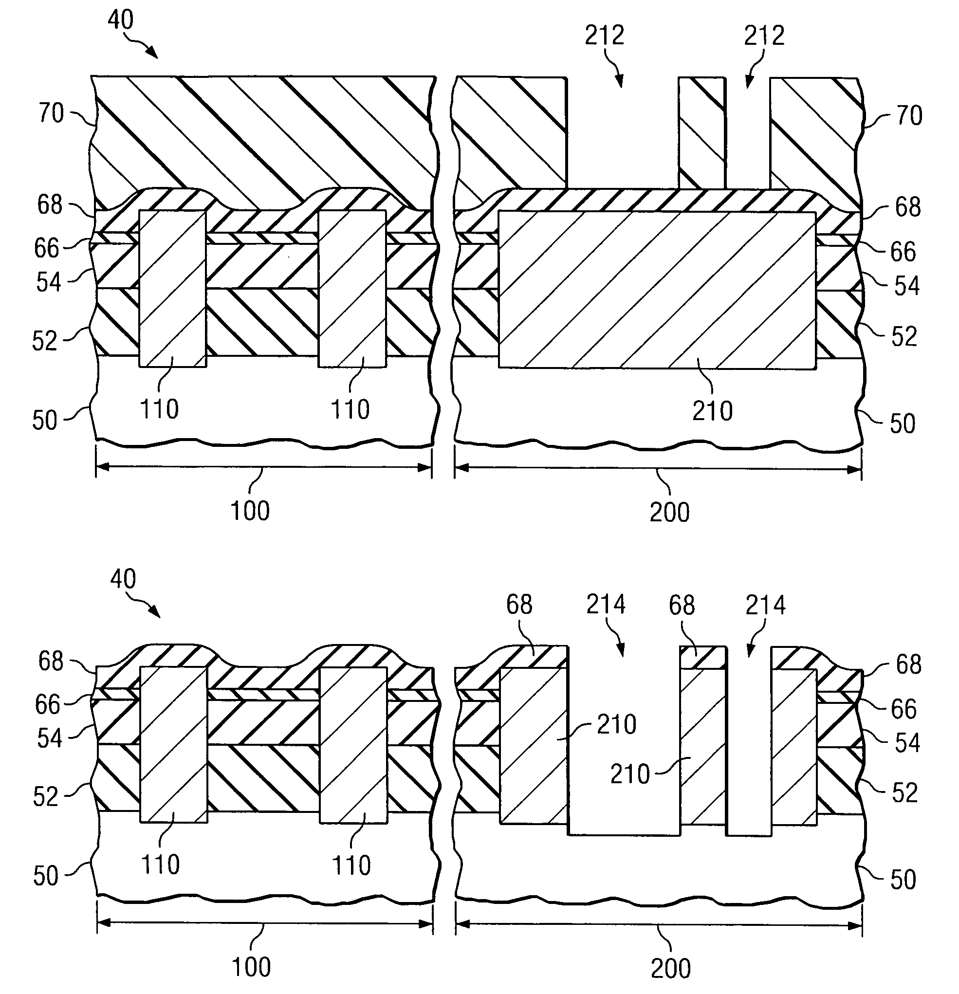
Figure 1 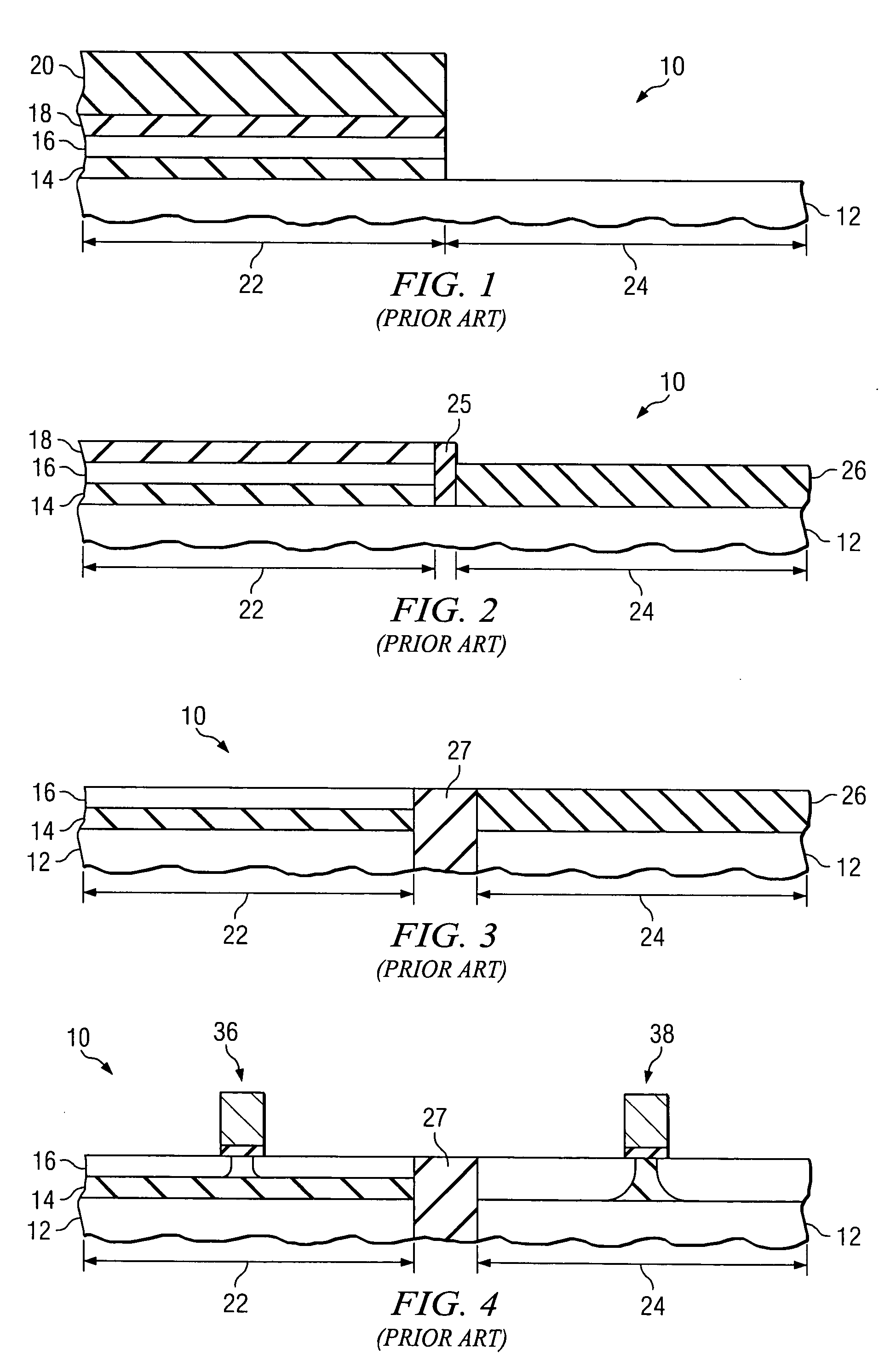
Figure 2 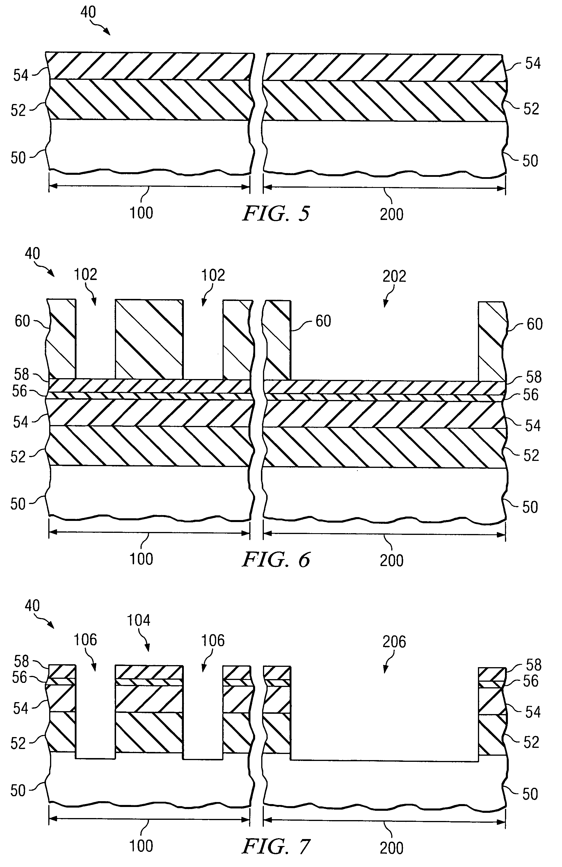
Figure 3
Abstract
Description
[0001] This application claims priority to provisional patent application Ser. No. 60 / 693,879, filed Jun. 24, 2005, entitled “High Performance Transistors with Hybrid Crystal Orientations,” which application is hereby incorporated herein by reference.TECHNICAL FIELD
[0002] The present invention relates to metal oxide semiconductor field effect transistors (MOSFETs), and more particularly to a method of fabricating a semiconductor structure having a hybrid crystal orientation and fabricating MOSFETs on the semiconductor structure.BACKGROUND
[0003] In present semiconductor technology, complementary metal oxide semiconductor (CMOS) devices, such as n-type field effect transistors (FETs) or NFETs, are typically fabricated on semiconductor wafers, such as silicon wafers that have a single crystal orientation, sometimes also referred to as direction. In particular, most of today's semiconductor devices are built on silicon substrates having a (100) crystal orientation.
[0004] Electrons are known...
Examples
Embodiment Construction
[0020]The making and using of the presently preferred embodiments are discussed in detail below. It should be appreciated, however, that the present invention provides many applicable inventive concepts that can be embodied in a wide variety of specific contexts. The specific embodiments discussed are merely illustrative of specific ways to make and use the invention, and do not limit the scope of the invention.
[0021]A novel method of forming a hybrid semiconductor structure having a hybrid crystal orientation and forming high performance MOSFETs on the hybrid semiconductor structure is illustrated in FIGS. 5 through 19. Throughout the various views and illustrative embodiments of the present invention, like reference numbers are used to designate like elements.
[0022]FIG. 5 illustrates a substrate 40 having a well-known SOI structure. The SOI structure includes a buried oxide (BOX) 52 on a semiconductor layer 50. A semiconductor layer 54 is on the BOX 52. In the preferred embodiment...