
Pixel and organic light emitting display using the same
a technology of organic light and display, applied in the field of pixels and organic light emitting display, can solve the problems of reducing the aperture ratio of the corresponding pixels, increasing power consumption, etc., and achieve the effect of reducing or minimizing the number of transistors positioned in the leakage current path, reducing or minimizing the leakage curren
Patent Information
- Authority / Receiving Office
- US · United States
- Patent Type
- Patents(United States)
- Current Assignee / Owner
- Publication Date
- 2014-07-22
Smart Images
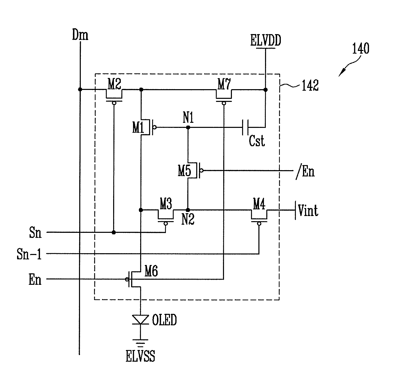
Figure 1 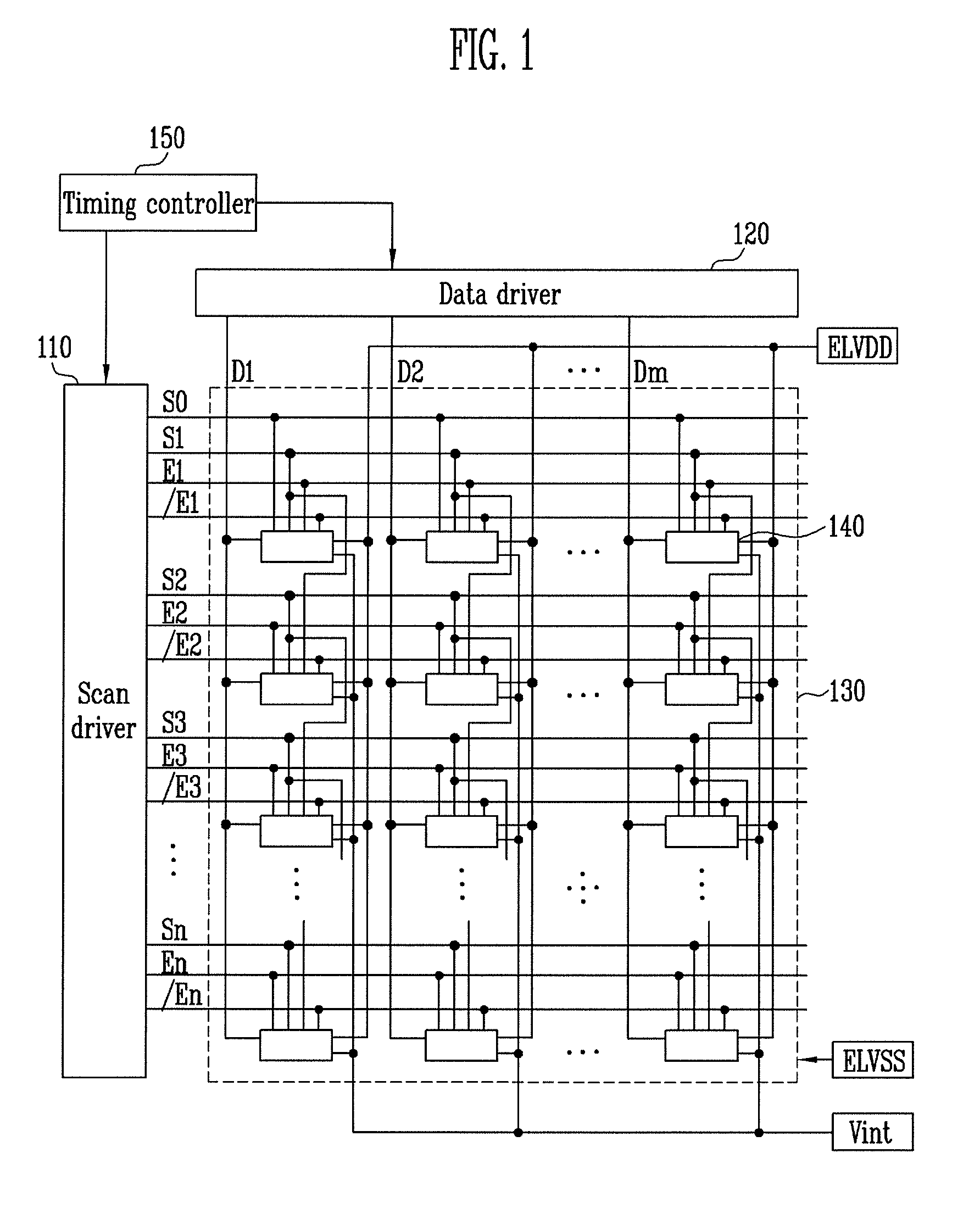
Figure 2 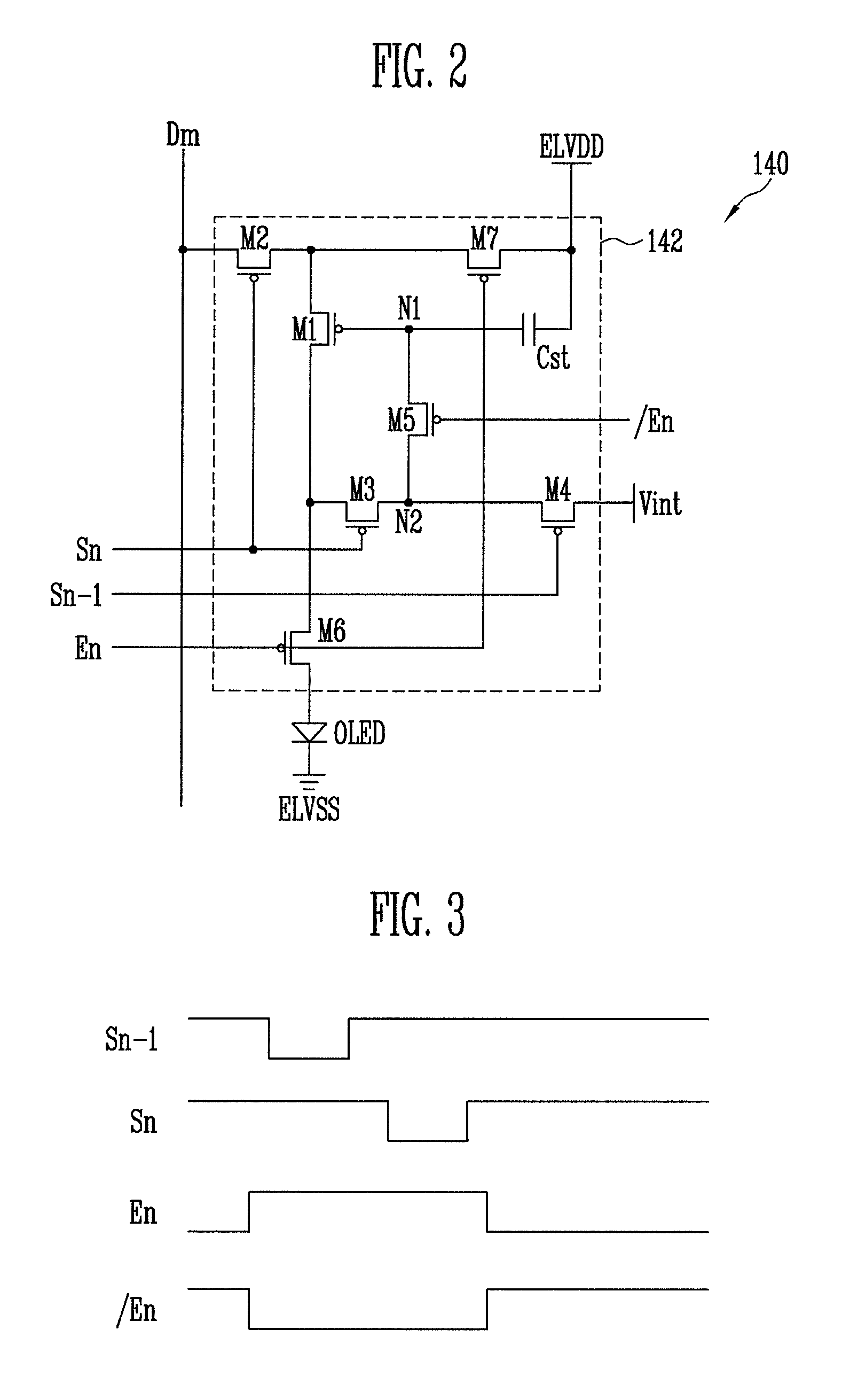
Figure 3
Abstract
Description
CROSS-REFERENCE TO RELATED APPLICATION
[0001] This application claims priority to and the benefit of Korean Patent Application No. 10-2010-0077315, filed on Aug. 11, 2010, in the Korean Intellectual Property Office, the entire content of which is incorporated herein by reference.BACKGROUND
[0002] 1. Field
[0003] Aspects of embodiments according to the present invention relate to a pixel and an organic light emitting display using the pixel.
[0004] 2. Description of the Related Art
[0005] Recently, various flat panel displays (FPDs) having reduced weight and volume when compared to those of cathode ray tube (CRT) devices have been developed. The FPDs include a liquid crystal display (LCD), a field emission display (FED), a plasma display panel (PDP), and an organic light emitting display.
[0006] Among the FPDs, the organic light emitting display displays images using organic light emitting diodes (OLEDs) that generate light by re-combination of electrons and holes. The organic light emitting dis...
Examples
first embodiment
[0049]FIG. 2 is a view illustrating the pixel 140 of FIG. 1. In FIG. 2, for convenience sake, the pixel 140 coupled to the (n-1)th scan line Sn-1, the nth scan line Sn, and the mth data line Dm will be described.
[0050]Referring to FIG. 2, the pixel 140 includes an OLED and a pixel circuit 142 coupled to the data line Dm, the scan lines Sn-1 and Sn, the emission control line En, and the inverted emission control line / En to control the amount of current supplied to the OLED.
[0051]An anode electrode of the OLED is coupled to the pixel circuit 142 and a cathode electrode of the OLED is coupled to the second power source ELVSS. The OLED generates light with brightness (for example, predetermined brightness) to correspond to the current supplied from the pixel circuit 142.
[0052]The pixel circuit 142 controls the amount of current supplied to the OLED to correspond to the data signal. Therefore, the pixel circuit 142 includes first to seventh transistors M1 to M7 and a storage capacitor C...
second embodiment
[0072]FIG. 4 is a view illustrating the pixel 140 of FIG. 1. In FIG. 4, the same elements as the elements of FIG. 2 are denoted by the same reference numerals, and detailed description thereof will not be repeated.
[0073]Referring to FIG. 4, the pixel 140 includes an OLED and a pixel circuit 143 coupled to the data line Dm, the scan lines Sn-1 and Sn, the emission control line En, and the inverted emission control line / En to control the amount of current supplied to the OLED.
[0074]The pixel circuit 143 controls the amount of current supplied to the OLED to correspond to the data signal. The pixel circuit 143 includes a plurality of fifth transistors M5_1 and M5_2 serially coupled between the first node N1 and the second node N2. The gate electrodes of the fifth transistors M5_1 and M5_2 are coupled to the inverted emission control line / En. The fifth transistors M5_1 and M5_2 are turned on when the inverted emission control signal is supplied to the inverted emission control line / E...
third embodiment
[0076]FIG. 5 is a view illustrating the pixel 140 of FIG. 1. In FIG. 5, the same elements as the elements of FIG. 2 are denoted by the same reference numerals, and detailed description thereof will not be repeated.
[0077]Referring to FIG. 5, the pixel 140 includes an OLED and a pixel circuit 144 coupled to the data line Dm, the scan lines Sn-1 and Sn, the emission control line En, and the inverted emission control line / En to control the amount of current supplied to the OLED.
[0078]The pixel circuit 144 controls the amount of current supplied to the OLED to correspond to the data signal. The pixel circuit 144 further includes an eighth transistor M8 coupled between the second node N2 and a reference power source Vref. The eighth transistor M8 is turned off when the emission control signal is supplied to the emission control line En and is turned on in the other cases.
[0079]That is, the eighth transistor M8 is turned on when the OLED emits light to supply a voltage of the reference po...