

ALD Seed Layer Engineering For Subsequent Electroplating Steps
AUG 28, 20259 MIN READ
Generate Your Research Report Instantly with AI Agent
PatSnap Eureka helps you evaluate technical feasibility & market potential.
ALD Seed Layer Technology Background and Objectives
Atomic Layer Deposition (ALD) seed layer technology has evolved significantly over the past two decades, transforming from an experimental technique to a critical process in advanced semiconductor manufacturing. Initially developed in the 1970s as a variant of Chemical Vapor Deposition (CVD), ALD gained prominence in the early 2000s when the semiconductor industry faced challenges with traditional physical vapor deposition (PVD) methods at sub-100nm nodes. The unique ability of ALD to deposit ultra-thin, highly conformal films with precise thickness control at the atomic level has made it indispensable for modern device fabrication.
The evolution of ALD seed layers has been driven by the continuous miniaturization of semiconductor devices following Moore's Law. As feature sizes decreased below 22nm, conventional PVD techniques struggled to provide adequate step coverage in high-aspect-ratio structures, creating reliability concerns for subsequent electroplating processes. ALD emerged as a solution by offering superior conformality even in complex 3D structures with aspect ratios exceeding 100:1, enabling void-free metallization.
Recent technological trends have focused on developing ALD processes for an expanded range of materials beyond the traditional copper seed layers. This includes noble metals like ruthenium, platinum, and palladium, as well as cobalt, which has gained attention as a potential replacement for copper in advanced nodes. The industry has also witnessed significant improvements in ALD precursor chemistry, enabling lower deposition temperatures, faster cycle times, and reduced impurity incorporation.
The primary objective of ALD seed layer engineering is to create an optimal interface between the diffusion barrier layer and the bulk conductor material deposited by electroplating. This interface must provide excellent adhesion, uniform nucleation for subsequent electroplating, low electrical resistance, and resistance to electromigration. Additionally, as device dimensions continue to shrink, the seed layer must maintain these properties while becoming increasingly thinner to maximize the volume available for the bulk conductor.
Another critical goal is to develop ALD processes compatible with emerging device architectures, including Gate-All-Around (GAA) transistors, 3D NAND, and advanced logic interconnects. These structures present unprecedented challenges in terms of aspect ratio, feature complexity, and material compatibility that push the boundaries of conventional deposition techniques.
Looking forward, the industry aims to integrate ALD seed layer technology with other advanced processes, such as selective deposition and area-selective ALD, to enable bottom-up filling approaches that could potentially eliminate the need for subsequent planarization steps. This integration represents a paradigm shift in metallization strategies and aligns with broader industry efforts toward more efficient, less wasteful manufacturing processes.
Market Analysis for ALD Seed Layer Applications
The global market for ALD seed layer applications is experiencing robust growth, driven primarily by the semiconductor and electronics industries. Current market size is estimated at $2.3 billion in 2023, with projections indicating a compound annual growth rate (CAGR) of 11.7% through 2028. This growth trajectory is supported by increasing demand for miniaturized electronic components and advanced packaging technologies that require precise thin film deposition capabilities.
The semiconductor industry represents the largest market segment, accounting for approximately 65% of total ALD seed layer applications. This dominance stems from the critical role seed layers play in enabling reliable metallization processes for increasingly complex chip architectures. The transition to sub-7nm nodes has particularly accelerated adoption, as traditional PVD methods struggle to provide adequate step coverage at these dimensions.
Advanced packaging applications constitute the second-largest market segment at 18%, followed by MEMS devices at 9%. The remaining market share is distributed across various emerging applications including medical devices, energy storage solutions, and optical components. Geographically, Asia-Pacific leads with 58% market share, followed by North America (24%) and Europe (15%).
Customer demand is increasingly focused on seed layers that can enable higher aspect ratio features while maintaining excellent adhesion properties and low resistivity. Market research indicates that 73% of end-users prioritize seed layer uniformity as the most critical performance parameter, followed by adhesion strength (68%) and resistivity (61%).
The competitive landscape features both established equipment manufacturers and specialty materials suppliers. Equipment providers are focusing on integrated solutions that combine ALD seed layer deposition with subsequent electroplating capabilities, offering customers streamlined production workflows. Materials suppliers are developing novel precursors designed specifically for seed layer applications, with emphasis on copper, ruthenium, and cobalt chemistries.
Market challenges include high equipment costs, which remain a significant barrier to adoption for smaller manufacturers. Additionally, process integration complexities when transitioning from traditional PVD seed layers to ALD alternatives represent a technical hurdle that impacts market penetration rates. Despite these challenges, the overall market outlook remains positive, supported by the irreversible trend toward device miniaturization and the superior performance characteristics of ALD-based seed layers for advanced electroplating processes.
Current Challenges in ALD Seed Layer Engineering
Despite significant advancements in ALD seed layer technology, several critical challenges persist that impede optimal performance in subsequent electroplating processes. The fundamental issue of nucleation control remains problematic, particularly on complex 3D structures with high aspect ratios. Current ALD processes often struggle to achieve uniform nucleation across varying surface chemistries, resulting in inconsistent seed layer formation that negatively impacts electroplating quality.
Adhesion limitations represent another significant challenge, especially at the interface between the seed layer and underlying substrates. The weak adhesion often leads to delamination during electroplating processes, causing reliability concerns in final devices. This issue becomes more pronounced as feature sizes continue to shrink in advanced semiconductor nodes.
Conformality in high-aspect-ratio structures presents persistent difficulties, with current ALD seed layer technologies showing diminishing performance as aspect ratios exceed 10:1. The challenge intensifies with the industry's push toward more complex 3D architectures, where complete and uniform coverage becomes increasingly difficult to achieve, particularly at the bottom of deep trenches and vias.
Resistivity management remains problematic, as ultra-thin ALD seed layers typically exhibit higher resistivity compared to their thicker counterparts. This increased resistivity can lead to non-uniform current distribution during electroplating, resulting in thickness variations and potential void formation. The trade-off between layer thinness for conformality and thickness for conductivity presents a significant engineering dilemma.
Integration challenges with subsequent processing steps also persist. ALD seed layers must maintain stability during pre-electroplating cleaning steps and resist oxidation when exposed to ambient conditions. Current solutions often require additional protective layers or specialized handling, adding complexity to manufacturing processes.
Material selection constraints further complicate ALD seed layer engineering. While copper remains the industry standard for interconnects, finding suitable precursors for direct copper ALD with appropriate nucleation characteristics continues to challenge researchers. Alternative materials like ruthenium and cobalt show promise but introduce new integration challenges related to adhesion and interface chemistry.
Scalability and throughput limitations affect industrial implementation, as traditional ALD processes are inherently slower than competing deposition methods. Although spatial ALD and batch processing have improved throughput, they often compromise conformality or uniformity, particularly for leading-edge applications requiring precise control over seed layer properties.
Current ALD Seed Layer Solutions for Electroplating
01 ALD seed layer deposition techniques for semiconductor devices
Atomic Layer Deposition (ALD) techniques are used to deposit seed layers for semiconductor device fabrication. These techniques allow for precise control over layer thickness and composition, enabling the formation of uniform and conformal seed layers even in high-aspect-ratio structures. The ALD process involves sequential self-limiting surface reactions that result in atomic-level control of film growth, which is crucial for advanced semiconductor manufacturing processes.- ALD seed layer deposition techniques for semiconductor devices: Atomic Layer Deposition (ALD) techniques are used to deposit seed layers for semiconductor devices with precise thickness control. These methods enable the formation of uniform, conformal seed layers on complex structures with high aspect ratios. The ALD process involves sequential self-limiting surface reactions that allow atomic-level control of film growth, resulting in excellent step coverage and conformality even in deep trenches and vias. These seed layers serve as a foundation for subsequent material growth or electroplating processes.
- Seed layer engineering for improved adhesion and film properties: Engineering seed layers through composition control and surface treatments enhances adhesion between different materials and improves the properties of subsequently deposited films. By carefully selecting seed layer materials and modifying their surface characteristics, issues such as delamination and poor nucleation can be addressed. Techniques include surface functionalization, interface engineering, and the use of adhesion promoters to create strong bonds between the substrate and subsequent layers, resulting in better film quality and device performance.
- Multi-layer seed structures for enhanced film growth: Multi-layer seed structures consisting of different materials are designed to optimize film growth in various applications. These engineered stacks combine the beneficial properties of different materials to overcome limitations of single-material seed layers. The first layer typically provides adhesion to the substrate, while subsequent layers facilitate nucleation and growth of the target film. This approach enables better control over crystallinity, grain structure, and other physical properties of the deposited films, leading to improved device performance.
- ALD seed layers for memory and logic device applications: Specialized ALD seed layers are developed for advanced memory and logic device applications, including DRAM, flash memory, and high-k metal gate transistors. These seed layers facilitate the growth of subsequent functional materials with specific electrical properties. The precise thickness control and conformality of ALD-deposited seed layers are particularly valuable for scaled devices with demanding dimensional requirements. The seed layer composition and structure are tailored to enhance device performance metrics such as switching speed, retention time, and reliability.
- Novel materials and processes for ALD seed layer engineering: Research on novel materials and innovative processes expands the capabilities of ALD seed layer engineering. These advancements include the use of new precursors, plasma-enhanced ALD techniques, and hybrid deposition approaches that combine ALD with other methods. Novel seed layer materials such as ternary compounds, doped films, and nanocomposites offer enhanced functionality beyond traditional options. These innovations enable seed layers with improved electrical conductivity, barrier properties, and compatibility with subsequent processing steps.
02 Seed layer engineering for improved thin film growth
Seed layer engineering involves the manipulation of seed layer properties to enhance subsequent thin film growth. By carefully controlling the composition, thickness, and microstructure of the seed layer, the crystallinity, orientation, and other properties of the overlying films can be optimized. This approach is particularly important for applications requiring specific film characteristics, such as in memory devices, transistors, and other electronic components.Expand Specific Solutions03 Metal and metal nitride seed layers for interconnect structures
Metal and metal nitride seed layers are critical components in the fabrication of interconnect structures in integrated circuits. These seed layers, often deposited using ALD, provide a foundation for subsequent metal deposition processes such as electroplating. Materials like tantalum, titanium, ruthenium, and their nitrides are commonly used as seed layers to improve adhesion, prevent diffusion, and enhance the electrical properties of interconnect structures.Expand Specific Solutions04 ALD seed layers for advanced memory applications
ALD seed layers play a crucial role in the fabrication of advanced memory devices such as DRAM, MRAM, and phase-change memory. These seed layers help control the growth and properties of functional materials in memory cells, including ferroelectric materials, magnetic materials, and phase-change materials. The precise control offered by ALD enables the scaling of memory devices while maintaining or improving their performance characteristics.Expand Specific Solutions05 Seed layer surface modification and treatment
Surface modification and treatment of seed layers are essential for optimizing subsequent film growth. Techniques such as plasma treatment, annealing, and surface functionalization can be employed to modify the surface properties of seed layers, including surface energy, roughness, and chemical reactivity. These modifications can significantly impact the nucleation, adhesion, and growth mode of subsequent layers, leading to improved device performance and reliability.Expand Specific Solutions
Key Industry Players in ALD and Electroplating
The ALD seed layer engineering for electroplating market is currently in a growth phase, with increasing adoption across semiconductor and electronics manufacturing. The market is expanding rapidly due to miniaturization trends in microelectronics, with an estimated value exceeding $500 million annually. Technologically, Applied Materials, ASM International, and Tokyo Electron lead with mature ALD solutions, while GlobalFoundries and Samsung Electro-Mechanics have developed advanced implementation strategies. QUALCOMM and Huawei represent key end-users driving requirements. Emerging players like ACM Research and Atotech are gaining traction with specialized electroplating solutions. The technology shows varying maturity levels across applications, with semiconductor interconnects being most advanced, while emerging areas like advanced packaging remain in development phases, creating competitive differentiation opportunities.
Applied Materials, Inc.
Technical Solution: Applied Materials has developed advanced ALD seed layer technology specifically engineered for subsequent electroplating processes. Their Endura® platform incorporates PVD-ALD hybrid approaches that enable ultra-thin, highly conformal seed layers for advanced packaging and interconnect applications. The company's technology utilizes precise control of nucleation processes through specialized ALD precursors and plasma enhancement techniques to achieve seed layers as thin as 2-3nm while maintaining excellent step coverage (>95%) in high aspect ratio features. Applied Materials' solution includes multi-step ALD processes that first deposit an adhesion layer (typically TiN or TaN) followed by a highly conductive Cu or Co seed layer, optimized for void-free gap filling during subsequent electroplating. Their technology addresses critical challenges in advanced node manufacturing by enabling seed layers that provide uniform nucleation sites for electroplating while minimizing overhang formation at feature openings.
Strengths: Superior conformality in high aspect ratio features; excellent adhesion properties; precise thickness control at nanometer scale; compatibility with various substrate materials; reduced overhang formation. Weaknesses: Higher cost compared to traditional PVD-only approaches; slower throughput than conventional methods; requires specialized precursors that may have limited availability.
ASM International NV
Technical Solution: ASM International has pioneered advanced ALD seed layer solutions through their Emerald™ and Eagle® platforms specifically designed for electroplating applications. Their technology employs thermal and plasma-enhanced ALD processes to deposit ultra-thin (2-5nm) seed layers with exceptional conformality (>98%) in high aspect ratio structures. ASM's approach involves multi-layer stacks where an initial adhesion layer (typically TiN) is followed by a nucleation enhancement layer and finally a highly conductive seed layer optimized for subsequent electroplating. Their proprietary precursor chemistry enables selective deposition capabilities, allowing targeted seed layer formation only where needed. ASM has demonstrated successful implementation of Ru-based seed layers as alternatives to traditional Cu seeds, offering superior resistance to oxidation and improved reliability. Their technology incorporates in-situ surface treatment capabilities that enhance nucleation density and adhesion properties, resulting in void-free filling during electroplating even for features below 10nm.
Strengths: Industry-leading conformality in complex 3D structures; excellent nucleation properties for subsequent electroplating; capability for selective deposition; compatibility with various substrate materials including advanced dielectrics. Weaknesses: Higher cost of ownership compared to traditional methods; throughput limitations for high-volume manufacturing; specialized precursor requirements that may impact supply chain flexibility.
Critical Patents and Innovations in ALD Seed Engineering
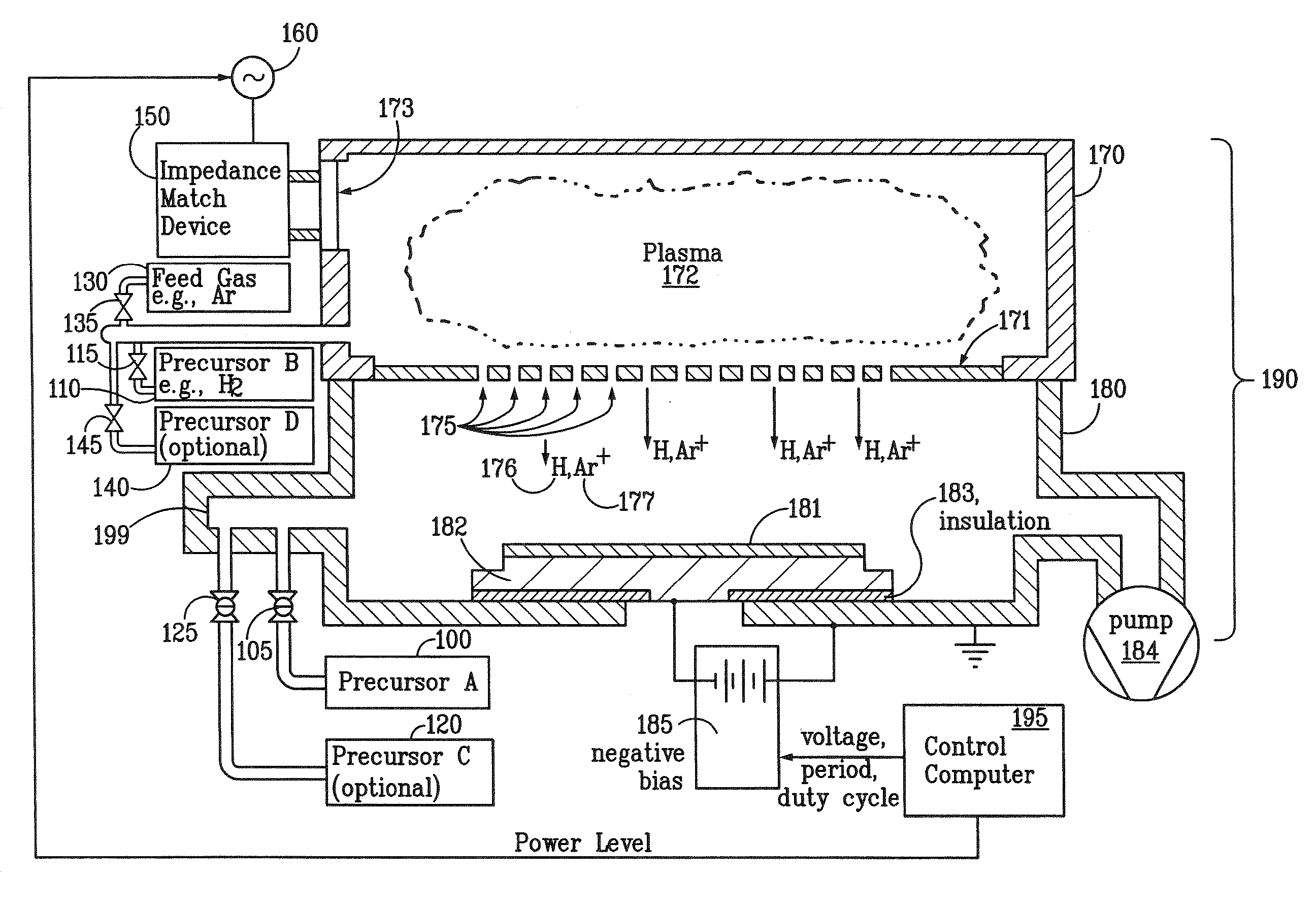
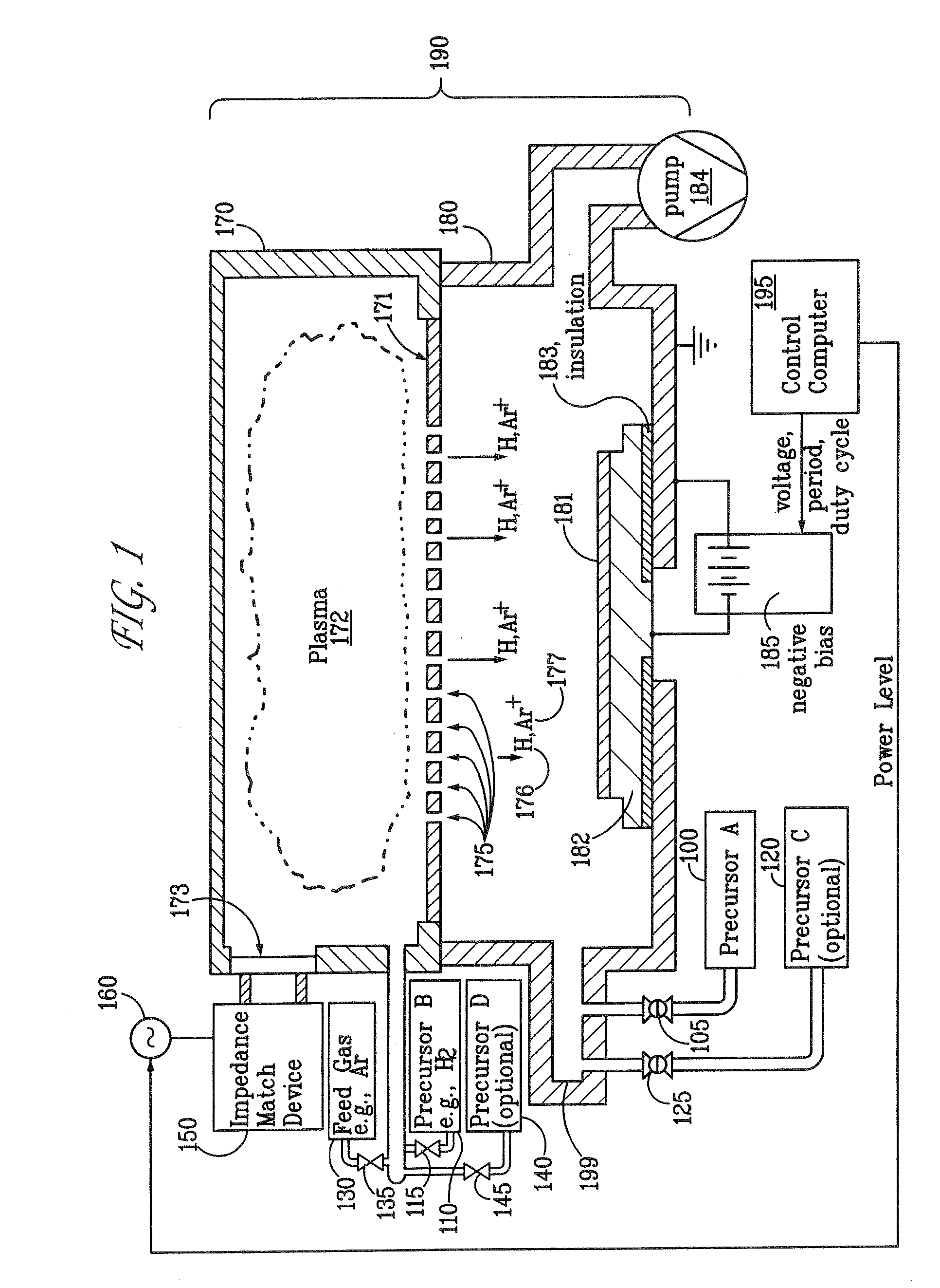
System for Depositing a Film by Modulated Ion-Induced Atomic Layer Deposition (MII-ALD)
PatentInactiveUS20110017139A1
Innovation
- The modulated ion-induced atomic layer deposition (MII-ALD) method uses ion bombardment as a non-thermal activation source to drive the deposition reaction, employing a microwave-generated plasma to generate ions and radicals efficiently, allowing for lower substrate temperatures and faster deposition rates, while maintaining high film purity and adhesion properties.
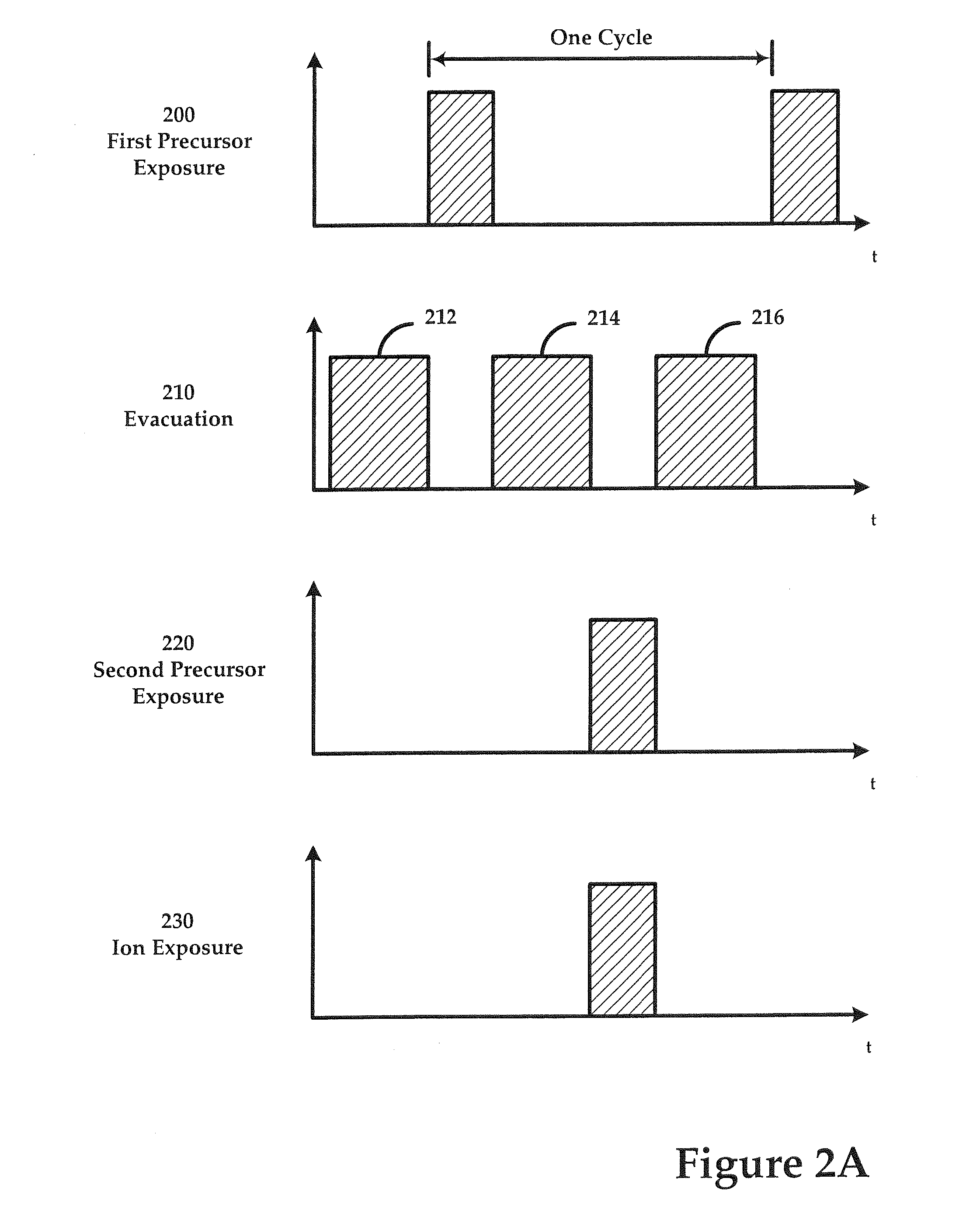
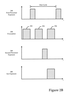
Combinatorial Plasma Enhanced Deposition Techniques
PatentInactiveUS20150144061A1
Innovation
- Combinatorial plasma enhanced deposition techniques are employed, allowing for the variation of parameters such as plasma presence, precursor types, and exposure times across different regions of a substrate, enabling the simultaneous exploration and evaluation of multiple materials and processes, thereby optimizing deposition conditions.


Material Compatibility and Interface Engineering
Material compatibility and interface engineering represent critical aspects in ALD seed layer development for electroplating applications. The interaction between the substrate, seed layer, and subsequent electroplated material determines the overall performance and reliability of the final structure. Careful consideration of material selection is essential to ensure strong adhesion, minimal stress, and optimal electrical properties at interfaces.
The compatibility between ALD seed layers and underlying substrates presents significant challenges, particularly when dealing with diverse substrate materials such as silicon, glass, polymers, or ceramics. Each substrate exhibits unique surface chemistry that influences nucleation behavior during ALD processes. For instance, hydroxyl-terminated surfaces facilitate efficient nucleation for oxide-based seed layers, while hydrogen-terminated surfaces may require additional surface modification steps to achieve uniform coverage.
Interface engineering techniques have evolved substantially to address adhesion issues between dissimilar materials. Approaches include the implementation of adhesion-promoting interlayers, surface activation treatments, and gradient composition layers that provide a transitional interface between materials with different properties. These techniques help mitigate stress concentration at interfaces and prevent delamination during subsequent processing steps or during device operation.
Chemical compatibility between the ALD seed layer and electroplating bath chemistry represents another critical consideration. Certain seed layer materials may undergo undesired reactions or dissolution when exposed to electroplating solutions, compromising their functionality. Noble metal seed layers like ruthenium and platinum demonstrate excellent chemical stability in most electroplating environments, while copper seed layers may require protective treatments to prevent oxidation before electroplating.
Thermal expansion coefficient matching between layers has emerged as an important factor in applications involving thermal cycling. Mismatched thermal expansion can induce mechanical stress during temperature fluctuations, potentially leading to cracking or delamination. Engineered interface layers with intermediate expansion coefficients can help distribute stress and maintain structural integrity across temperature ranges.
Recent advances in interface engineering include atomic-level control of interface composition through sequential ALD processes, enabling the creation of atomically abrupt or gradually changing interfaces as required by specific applications. Additionally, post-deposition treatments such as annealing in controlled atmospheres have proven effective in promoting interfacial diffusion and chemical bonding, enhancing adhesion strength between layers while maintaining the desired electrical characteristics essential for subsequent electroplating steps.
Environmental Impact and Sustainability Considerations
The integration of ALD seed layer technology with electroplating processes presents significant environmental and sustainability implications that merit careful consideration. Traditional electroplating methods have historically been associated with substantial environmental concerns, including high water consumption, toxic chemical usage, and hazardous waste generation. ALD seed layer engineering offers promising pathways to mitigate these impacts through more precise material deposition and reduced chemical requirements.
When examining the environmental footprint of ALD seed layer processes, water consumption emerges as a critical factor. Conventional electroplating typically demands large volumes of water for rinsing and processing steps. ALD seed layer technology can reduce water requirements by up to 30-40% through more targeted deposition that minimizes subsequent cleaning needs. This water conservation aspect becomes increasingly valuable as manufacturing facilities face growing water scarcity challenges and stricter regulatory frameworks regarding water usage.
Chemical efficiency represents another substantial sustainability advantage of ALD seed layer engineering. The atomic-level precision inherent to ALD processes enables significant reductions in precursor material consumption compared to conventional seeding methods. Studies indicate that ALD approaches can achieve up to 95% material utilization efficiency, dramatically reducing chemical waste streams. Furthermore, the ability to engineer ultra-thin seed layers (often <10nm) minimizes the quantity of precious metals required, addressing resource scarcity concerns for materials like ruthenium, platinum, and palladium.
Energy consumption patterns also differ significantly between traditional and ALD-based approaches. While ALD processes typically operate at elevated temperatures (150-350°C), their precise nature and shorter subsequent electroplating requirements can yield net energy savings of 15-25% across the complete manufacturing cycle. The development of low-temperature ALD variants (80-120°C) further enhances these sustainability benefits, particularly for temperature-sensitive applications.
Waste management considerations strongly favor ALD seed layer implementation. The technology produces significantly lower volumes of metal-containing waste streams and spent solutions compared to conventional electroless deposition methods. This reduction translates to decreased environmental remediation costs and reduced environmental liability for manufacturing operations. Additionally, the elimination or substantial reduction of formaldehyde and other environmentally problematic reducing agents commonly used in electroless processes represents a meaningful advancement in green chemistry principles.
Looking forward, life cycle assessment (LCA) studies indicate that ALD seed layer engineering, when optimized for specific electroplating applications, can reduce the overall environmental impact by 20-35% compared to conventional approaches. This improvement encompasses reduced carbon footprint, decreased water pollution potential, and diminished resource depletion metrics. As sustainability becomes increasingly central to manufacturing strategy, these environmental advantages position ALD seed layer technology as an important contributor to more environmentally responsible electronics and semiconductor production.
Unlock deeper insights with PatSnap Eureka Quick Research — get a full tech report to explore trends and direct your research. Try now!
Generate Your Research Report Instantly with AI Agent
Supercharge your innovation with PatSnap Eureka AI Agent Platform!