Integration Of SALD With Laser Patterning For Device Fabrication
AUG 28, 20259 MIN READ
Generate Your Research Report Instantly with AI Agent
Patsnap Eureka helps you evaluate technical feasibility & market potential.
SALD-Laser Patterning Integration Background and Objectives
Spatial Atomic Layer Deposition (SALD) represents a significant advancement in thin film deposition technology, evolving from conventional Atomic Layer Deposition (ALD) techniques that emerged in the 1970s. While traditional ALD offers exceptional film uniformity and thickness control at the atomic scale, its inherently slow processing speed has limited industrial adoption. SALD addresses this limitation by spatially separating precursor gases rather than temporally sequencing them, enabling continuous deposition and dramatically increasing throughput by 10-100 times compared to conventional ALD.
Laser patterning technology has developed in parallel, progressing from basic material ablation techniques to sophisticated direct-write methods capable of nanometer-scale precision. The evolution of ultrafast lasers with femtosecond pulses has enabled cold ablation processes that minimize thermal damage to surrounding materials, making them increasingly compatible with sensitive electronic and photonic device fabrication.
The integration of these two technologies represents a convergence of complementary capabilities that addresses critical manufacturing challenges in next-generation electronics, photonics, and energy devices. This technological synergy aims to combine SALD's ability to create high-quality conformal thin films with laser patterning's precision in material removal and modification, potentially enabling single-tool fabrication processes that previously required multiple steps and equipment.
The primary objective of this integration is to develop a seamless manufacturing approach that maintains the advantages of both technologies while overcoming their individual limitations. Specifically, we aim to achieve in-line selective deposition and patterning capabilities that eliminate the need for traditional photolithography steps, thereby reducing process complexity, material waste, and production costs.
Additional technical goals include developing precise alignment systems between deposition and patterning processes, optimizing laser parameters to avoid damage to underlying SALD films, and creating integrated control systems that synchronize both processes for maximum throughput and yield. The ultimate vision is to enable roll-to-roll or large-area processing of complex device architectures with nanoscale precision.
From an applications perspective, this integration targets several high-value markets including flexible electronics, transparent conductive electrodes, photovoltaics, solid-state batteries, and advanced sensing devices. Each of these applications benefits from the ability to create precisely patterned thin films with exceptional quality and performance characteristics.
The technological trajectory suggests that successful integration could fundamentally transform manufacturing approaches for next-generation devices, potentially enabling new device architectures that are impractical or impossible with current fabrication techniques. This represents not merely an incremental improvement in existing processes, but potentially a paradigm shift in how complex functional devices are manufactured.
Market Analysis for Integrated SALD-Laser Fabrication Solutions
The global market for integrated SALD-Laser patterning fabrication solutions is experiencing significant growth, driven by increasing demand for advanced electronic devices with higher performance and lower production costs. This integrated technology combines the precision of Spatial Atomic Layer Deposition (SALD) with the versatility of laser patterning, creating a powerful solution for next-generation device manufacturing.
The current market size for SALD-Laser integrated systems is estimated at $2.3 billion, with projections indicating growth to $5.7 billion by 2028, representing a compound annual growth rate of 19.8%. This growth trajectory is primarily fueled by expanding applications in semiconductor manufacturing, display technologies, and emerging flexible electronics sectors.
Consumer electronics remains the dominant application segment, accounting for approximately 42% of the market share. The semiconductor industry follows closely at 31%, with medical devices and automotive electronics representing 15% and 12% respectively. These percentages reflect the versatility of the integrated technology across multiple high-value manufacturing domains.
Geographically, Asia-Pacific leads the market with 48% share, driven by the concentration of electronics manufacturing facilities in countries like South Korea, Japan, Taiwan, and China. North America holds 27% of the market, with Europe at 21%. The remaining 4% is distributed across other regions, indicating potential growth opportunities in emerging markets.
Key market drivers include the miniaturization trend in electronics, increasing demand for flexible and wearable devices, and the push for more environmentally sustainable manufacturing processes. The SALD-Laser integration addresses these needs by enabling precise material deposition with minimal waste while allowing for complex patterning without additional lithography steps.
Customer demand analysis reveals that manufacturers are particularly interested in systems offering higher throughput, improved layer uniformity, and enhanced pattern resolution. The ability to process temperature-sensitive substrates is becoming increasingly important as flexible electronics gain market traction.
Market challenges include the high initial investment cost for integrated systems, technical complexity requiring specialized operator training, and competition from established alternative technologies. However, the total cost of ownership analysis demonstrates that integrated SALD-Laser systems can provide up to 30% cost savings over conventional multi-step processes when considering material utilization, energy consumption, and reduced clean room requirements.
The market is expected to evolve toward more automated and AI-integrated systems, with predictive maintenance capabilities and real-time process optimization. This evolution will likely expand the addressable market by making the technology accessible to smaller manufacturers and research institutions.
Current Technological Landscape and Implementation Challenges
The integration of Spatial Atomic Layer Deposition (SALD) with laser patterning represents a significant advancement in device fabrication technology. Currently, this integration exists primarily in research environments, with limited commercial implementation. Leading research institutions in Europe, North America, and East Asia have demonstrated proof-of-concept devices, but widespread industrial adoption remains nascent.
SALD technology itself has evolved considerably over the past decade, transitioning from laboratory demonstrations to pilot-scale manufacturing systems. Companies like TNO (Netherlands), Beneq (Finland), and Meyer Burger (Switzerland) have developed atmospheric pressure SALD systems capable of high-throughput deposition. However, these systems typically operate as standalone units rather than integrated manufacturing solutions incorporating laser patterning.
The laser patterning landscape is more mature, with established technologies including excimer lasers, femtosecond lasers, and DPSS (Diode-Pumped Solid-State) lasers. Equipment manufacturers such as Coherent, IPG Photonics, and TRUMPF offer sophisticated laser systems with high precision and control. The challenge lies in effectively combining these two distinct technological ecosystems.
Key implementation challenges include process synchronization between deposition and patterning steps. SALD operates optimally under specific atmospheric conditions, while certain laser processes may require different environments, creating compatibility issues. Additionally, thermal management presents significant difficulties as laser processes generate localized heating that can affect the quality of SALD-deposited films or alter their properties.
Material compatibility represents another major hurdle. Not all materials deposited via SALD respond predictably to laser processing, with some exhibiting unwanted phase changes, delamination, or altered electrical/optical properties. This necessitates extensive material-specific process development and characterization.
Scaling challenges persist in achieving consistent results across larger substrate areas. Laboratory demonstrations typically involve small-area processing, while commercial applications require uniform performance across much larger dimensions. Variations in film thickness, composition, and laser energy distribution can lead to inconsistent device performance.
Equipment integration poses significant engineering challenges. Current manufacturing systems are not designed for seamless integration of these technologies, requiring custom engineering solutions that increase complexity and cost. The absence of standardized interfaces between SALD and laser systems further complicates integration efforts.
Finally, metrology and quality control systems capable of in-line monitoring for integrated SALD and laser processes remain underdeveloped. Real-time feedback mechanisms that could adjust process parameters to maintain optimal performance are largely absent in current implementations, limiting yield and consistency in fabricated devices.
Existing Integration Methodologies and Technical Approaches
01 SALD process integration with laser patterning techniques
Spatial Atomic Layer Deposition (SALD) can be integrated with laser patterning to create precisely defined structures on substrates. This combination allows for selective deposition of thin films in specific areas while using laser technology to pattern or modify the deposited materials. The integration enables high-throughput manufacturing of patterned thin films with nanoscale precision, which is particularly valuable for semiconductor and display applications.- SALD process integration with laser patterning techniques: Spatial Atomic Layer Deposition (SALD) can be integrated with laser patterning to create precisely defined structures. This combination allows for selective deposition of thin films in specific areas while using laser technology to pattern or modify the deposited materials. The integration enables high-throughput manufacturing of patterned thin films with nanoscale precision, which is particularly valuable for semiconductor and electronic device fabrication.
- Selective area deposition using SALD with laser-defined patterns: Laser patterning can be used to create templates or masks that guide the SALD process for selective area deposition. The laser defines regions where deposition should occur by modifying surface properties or creating physical barriers. This approach enables the fabrication of complex structures without traditional lithography steps, reducing manufacturing complexity and cost while maintaining high precision in the deposited patterns.
- Post-deposition laser processing of SALD films: After SALD deposition, laser processing can be applied to modify the properties of the deposited films. This includes laser annealing, ablation, or transformation of the material structure. The post-deposition laser treatment can enhance film crystallinity, remove unwanted portions, or create specific features in the deposited layers. This combination allows for precise control over both the deposition and subsequent modification of thin films.
- Materials and precursors for SALD with laser compatibility: Specific materials and precursors are developed for SALD processes that are compatible with subsequent laser patterning. These materials must withstand laser processing without degradation or can be selectively modified by laser exposure. The selection of appropriate precursors ensures optimal film properties after deposition and enables precise laser patterning with minimal damage to surrounding areas. This approach is particularly important for creating high-quality electronic and optical devices.
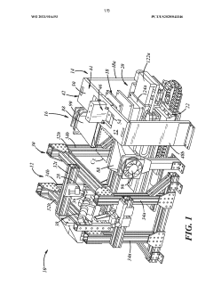
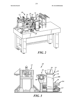
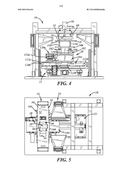
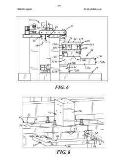
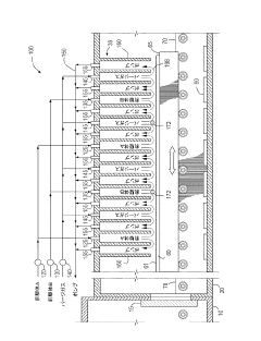
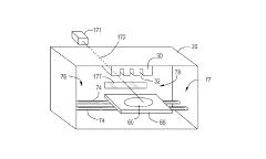
- Equipment and system integration for combined SALD and laser processing: Specialized equipment and systems have been developed to integrate SALD and laser processing in a single manufacturing line. These integrated systems allow for in-situ laser patterning during or immediately after the SALD process, minimizing handling and potential contamination. The equipment design focuses on precise alignment between deposition and laser patterning steps, controlled atmospheres, and high throughput for industrial applications. This integration enables more efficient production of patterned thin films for various applications.
02 Selective area deposition using laser-assisted SALD
Laser-assisted SALD techniques enable selective area deposition by using laser energy to activate specific regions of a substrate for material growth. The laser can be used to locally heat areas where deposition is desired, creating reaction sites for precursor molecules. This approach eliminates the need for traditional photolithography steps in some applications, reducing process complexity and manufacturing costs while maintaining high precision in pattern definition.Expand Specific Solutions03 Material modification and patterning post-SALD deposition
After SALD deposition of thin films, laser patterning can be employed to modify the material properties or remove selected areas. This post-deposition processing allows for the creation of complex structures by ablation, annealing, or chemical transformation of the deposited layers. The technique is particularly useful for creating functional devices such as thin-film transistors, sensors, and optoelectronic components with precise dimensional control.Expand Specific Solutions04 High-speed SALD with in-situ laser processing
Integrating high-speed SALD processes with in-situ laser processing enables continuous manufacturing workflows. This approach allows for immediate patterning or modification of deposited layers without breaking vacuum or transferring substrates between tools. The combination significantly improves throughput and reduces contamination risks, making it suitable for industrial-scale production of advanced electronic and photonic devices.Expand Specific Solutions05 Novel materials and structures enabled by SALD-laser hybrid processes
The combination of SALD and laser patterning enables the creation of novel materials and structures that would be difficult to achieve with either technology alone. These include gradient composition films, 3D nanostructures, and quantum confinement structures. The hybrid approach allows for precise control over material composition, crystallinity, and interface properties, opening new possibilities for next-generation electronic, energy storage, and sensing applications.Expand Specific Solutions
Industry Leaders in SALD and Laser Processing Integration
The integration of Spatial Atomic Layer Deposition (SALD) with laser patterning for device fabrication represents an emerging technological frontier currently in its early growth phase. The market is expanding rapidly, projected to reach significant scale as industries seek more efficient semiconductor and electronic device manufacturing processes. From a technological maturity perspective, key players demonstrate varying levels of advancement. Taiwan Semiconductor Manufacturing Co. (TSMC) and Samsung Electronics lead commercial implementation, while research institutions like Nanjing University of Aeronautics & Astronautics and Luxembourg Institute of Science & Technology drive fundamental innovation. Companies including Siemens, NVIDIA, and Xerox are developing specialized applications, while materials suppliers such as Solvay and SABIC provide essential components. This competitive landscape reflects a technology transitioning from research to industrial application, with significant potential for disruption in precision manufacturing.
Taiwan Semiconductor Manufacturing Co., Ltd.
Technical Solution: TSMC has developed an advanced integration approach combining SALD (Spatial Atomic Layer Deposition) with laser patterning for next-generation semiconductor device fabrication. Their technology utilizes a roll-to-roll SALD system for high-throughput deposition of ultrathin conformal films (5-20nm) on flexible substrates, achieving deposition rates up to 100 times faster than conventional ALD. The system incorporates multiple precursor heads with precise gas flow control to maintain separation between reactive chemicals while allowing continuous substrate movement. Following deposition, TSMC employs a proprietary laser patterning system using ultrafast femtosecond lasers that can create features down to 10μm without damaging underlying layers. This integrated approach enables direct patterning of functional materials like transparent conductive oxides and dielectrics without photolithography steps, significantly reducing manufacturing complexity and chemical waste.
Strengths: Dramatically higher throughput than conventional ALD; compatible with flexible substrates enabling new form factors; reduced manufacturing steps and chemical consumption; precise thickness control at nanometer scale. Weaknesses: Currently limited to feature sizes above 10μm; challenges with multi-layer alignment precision; higher initial capital investment compared to conventional techniques.
Samsung Electronics Co., Ltd.
Technical Solution: Samsung Electronics has pioneered an integrated SALD-laser patterning platform for advanced display and semiconductor manufacturing. Their system utilizes a multi-head SALD reactor design that enables high-speed deposition of uniform thin films across large-area substrates at atmospheric pressure. The SALD component achieves deposition rates of 1-2 nm/second while maintaining excellent film uniformity (±2%) and conformality over complex topographies. Samsung's innovation lies in their seamless integration of a high-precision laser patterning module directly within the SALD process line, enabling in-situ patterning without breaking vacuum or transferring substrates between tools. The laser system employs a galvanometer-based beam steering mechanism with multiple wavelength options (355nm, 532nm, and 1064nm) to optimize patterning for different material systems. This integrated approach allows for the fabrication of complex multilayer structures with precise alignment between layers, critical for advanced memory devices and displays.
Strengths: Seamless integration reduces handling steps and improves yield; atmospheric pressure operation lowers manufacturing costs; excellent thickness uniformity across large substrates; versatile material compatibility. Weaknesses: Higher initial equipment investment; challenges with ultra-high resolution patterning below 5μm; process optimization required for each new material system.
Key Patents and Research Breakthroughs in SALD-Laser Integration
Integrated electrohydrodynamic jet printing and spatial atomic layer deposition system for area-selective atomic layer deposition
PatentWO2021016493A1
Innovation
- An integrated electrohydrodynamic jet printing (E-jet printing) and spatial atomic layer deposition (SALD) system is developed, where E-jet printing is used to pattern inhibition materials with submicron resolution, combined with SALD for precise deposition of ALD films, and both processes are performed on the same substrate plate to enhance alignment and reduce downtime.
Apparatus and method for atomic layer deposition with horizontal laser
PatentInactiveJP2015517203A
Innovation
- The use of a deposition system with a gas distribution plate and laser sources to direct laser beams along elongated gas ports, facilitating precursor activation and reaction, and a substrate movement mechanism that enhances precursor exposure and reaction efficiency.
Materials Compatibility and Process Optimization Considerations
The integration of Spatial Atomic Layer Deposition (SALD) with laser patterning presents significant challenges and opportunities in materials compatibility and process optimization. When combining these two advanced manufacturing techniques, material selection becomes critical as not all substrates and thin film materials respond favorably to both processes.
For substrate materials, thermal stability during SALD processing followed by laser exposure is paramount. Materials such as glass, silicon, and certain polymers (polyimide, PET) demonstrate varying degrees of compatibility. Glass and silicon offer excellent thermal stability but may require specific surface treatments to enhance adhesion properties. Polymeric substrates, while offering flexibility advantages, must be carefully selected to withstand the thermal cycles of SALD without degradation before laser processing.
Thin film materials deposited via SALD must maintain their functional properties after laser patterning. Metal oxides (ZnO, Al2O3, TiO2) commonly used in SALD show good compatibility, though crystallization behavior may change during laser exposure. Metallic films often require precise laser parameters to avoid excessive heat-affected zones that could compromise adjacent structures.
Process sequencing represents another critical consideration. The optimal workflow—whether to perform SALD before laser patterning or vice versa—depends on specific material combinations and device requirements. Pre-patterning with lasers may create surface modifications that affect subsequent SALD film growth characteristics, while post-deposition patterning risks thermal damage to the deposited layers.
Temperature management during integration requires careful optimization. SALD typically operates at temperatures between 50-300°C depending on precursors and materials, while laser processes generate localized high temperatures. This thermal profile mismatch necessitates careful process design to prevent thermal stress, delamination, or unwanted diffusion between layers.
Atmosphere control presents additional challenges, as SALD requires specific gas environments while laser processing may generate particulates or require different atmospheric conditions. Integrated systems must address these competing requirements through specialized chamber designs or sequential processing with appropriate environmental transitions.
Scaling considerations further complicate integration efforts. While both technologies offer advantages for large-area manufacturing, their combined implementation requires synchronized scaling strategies to maintain process uniformity and throughput advantages across increasing substrate dimensions.
Scalability and Industrial Implementation Roadmap
The scalability of SALD (Spatial Atomic Layer Deposition) integration with laser patterning represents a critical factor for industrial adoption. Current laboratory-scale demonstrations have shown promising results, but transitioning to high-volume manufacturing requires significant engineering solutions. The throughput of SALD systems has already demonstrated substantial improvements over conventional ALD, with deposition rates up to 100 times faster, making it compatible with in-line production processes.
For industrial implementation, a phased approach is recommended. Short-term goals (1-2 years) should focus on optimizing existing SALD-laser integration for specific applications like thin-film transistors and solar cells, where immediate benefits can be realized. This includes standardizing interfaces between SALD and laser systems and developing automated handling systems for continuous processing.
Mid-term objectives (3-5 years) involve scaling up to larger substrate sizes and implementing roll-to-roll processing capabilities. This phase requires significant investment in equipment design to maintain process uniformity across larger areas while ensuring precise alignment between deposition and patterning steps. Atmospheric pressure operation of SALD makes this scaling more feasible than vacuum-based techniques.
Long-term implementation (5+ years) should target fully integrated production lines where SALD and laser patterning operate as synchronized components within comprehensive manufacturing systems. This includes real-time monitoring and feedback control systems to maintain quality during continuous operation.
Key technical challenges for industrial scaling include maintaining uniform gas flows over larger areas, ensuring consistent laser patterning quality at higher speeds, and developing robust in-line quality control methods. The capital expenditure for integrated systems remains high, though operational costs benefit from reduced material waste and energy consumption compared to traditional methods.
Industry partnerships between equipment manufacturers, material suppliers, and end-users will be essential to drive standardization and cost reduction. Several equipment manufacturers have already begun developing commercial-scale SALD systems with integrated patterning capabilities, though these remain primarily targeted at R&D applications rather than full production environments.
Return on investment calculations suggest that for high-value applications like flexible electronics and advanced photovoltaics, the payback period for integrated SALD-laser systems could be as short as 2-3 years, making them increasingly attractive for industrial implementation.
Unlock deeper insights with Patsnap Eureka Quick Research — get a full tech report to explore trends and direct your research. Try now!
Generate Your Research Report Instantly with AI Agent
Supercharge your innovation with Patsnap Eureka AI Agent Platform!